- 您现在的位置:买卖IC网 > PDF目录4239 > SST25WF040-40-5I-SAF-T (Microchip Technology)IC FLASH SER 4MB 40MHZ SPI 8SOIC PDF资料下载
参数资料
| 型号: | SST25WF040-40-5I-SAF-T |
| 厂商: | Microchip Technology |
| 文件页数: | 21/36页 |
| 文件大小: | 0K |
| 描述: | IC FLASH SER 4MB 40MHZ SPI 8SOIC |
| 标准包装: | 2,000 |
| 系列: | SST25 |
| 格式 - 存储器: | 闪存 |
| 存储器类型: | FLASH |
| 存储容量: | 4M (512K x 8) |
| 速度: | 40MHz |
| 接口: | SPI 串行 |
| 电源电压: | 1.65 V ~ 1.95 V |
| 工作温度: | -40°C ~ 85°C |
| 封装/外壳: | 8-SOIC(0.154",3.90mm 宽) |
| 供应商设备封装: | 8-SOIC |
| 包装: | 带卷 (TR) |
第1页第2页第3页第4页第5页第6页第7页第8页第9页第10页第11页第12页第13页第14页第15页第16页第17页第18页第19页第20页当前第21页第22页第23页第24页第25页第26页第27页第28页第29页第30页第31页第32页第33页第34页第35页第36页
�� �
�
�512� Kbit� /� 1� Mbit� /� 2� Mbit� /� 4� Mbit� 1.8V� SPI� Serial� Flash�
�A� Microchip� Technology� Company�
�SST25WF512� /� SST25WF010� /� SST25WF020� /� SST25WF040�
�Data� Sheet�
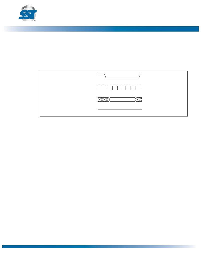
�Write-Disable� (WRDI)�
�The� Write-Disable� (WRDI)� instruction,� 04H,� resets� the� Write-Enable-Latch� bit� and� AAI� to� 0� disabling�
�any� new� Write� operations� from� occurring.� The� WRDI� instruction� will� not� terminate� any� programming�
�operation� in� progress.� Any� program� operation� in� progress� may� continue� up� to� T� BP� after� executing� the�
�WRDI� instruction.� CE#� must� be� driven� high� before� the� WRDI� instruction� is� executed.� See� Figure� 19� for�
�the� WRDI� instruction� sequence.�
�CE#�
�MODE� 3�
�0� 1� 2� 3� 4� 5� 6� 7�
�SCK�
�SI�
�SO�
�MODE� 0�
�04�
�MSB�
�HIGH� IMPEDANCE�
�1328� Fx19.0�
�Figure� 19:� Write� Disable� (WRDI)� Sequence�
�Enable-Write-Status-Register� (EWSR)�
�The� Enable-Write-Status-Register� (EWSR)� instruction� arms� the� Write-Status-Register� (WRSR)�
�instruction� and� opens� the� status� register� for� alteration.� The� Write-Status-Register� instruction� must� be�
�executed� immediately� after� the� execution� of� the� Enable-Write-Status-Register� instruction.� This� two-�
�step� instruction� sequence� of� the� EWSR� instruction� followed� by� the� WRSR� instruction� works� like� SDP�
�(software� data� protection)� command� structure� which� prevents� any� accidental� alteration� of� the� status�
�register� values.� CE#� must� be� driven� low� before� the� EWSR� instruction� is� entered� and� must� be� driven�
�high� before� the� EWSR� instruction� is� executed.� See� Figure� 20� for� EWSR� instruction� followed� by� WRSR�
�instruction.�
�Write-Status-Register� (WRSR)�
�The� Write-Status-Register� instruction� writes� new� values� to� the� BP1,� BP0,� and� BPL� bits� of� the� status�
�register.� CE#� must� be� driven� low� before� the� command� sequence� of� the� WRSR� instruction� is� entered�
�and� driven� high� before� the� WRSR� instruction� is� executed.� See� Figure� 20� for� EWSR� or� WREN� and�
�WRSR� instruction� sequences.�
�Executing� the� Write-Status-Register� instruction� will� be� ignored� when� WP#� is� low� and� BPL� bit� is� set� to�
�‘1’.� When� the� WP#� is� low,� the� BPL� bit� can� only� be� set� from� ‘0’� to� ‘1’� to� lock-down� the� status� register,� but�
�cannot� be� reset� from� ‘1’� to� ‘0’.� When� WP#� is� high,� the� lock-down� function� of� the� BPL� bit� is� disabled� and�
�the� BPL,� BP0,� and� BP1� bits� in� the� status� register� can� all� be� changed.� As� long� as� BPL� bit� is� set� to� ‘0’� or�
�WP#� pin� is� driven� high� (V� IH� )� prior� to� the� low-to-high� transition� of� the� CE#� pin� at� the� end� of� the� WRSR�
�instruction,� the� bits� in� the� status� register� can� all� be� altered� by� the� WRSR� instruction.� In� this� case,� a� sin-�
�?2011� Silicon� Storage� Technology,� Inc.�
�21�
�DS25016A�
�06/11�
�相关PDF资料 |
PDF描述 |
|---|---|
| 24FC128-I/MF | IC EEPROM 128KBIT 1MHZ 8DFN |
| XC4VFX12-12SFG363C | IC FPGA VIRTEX-4 FX 12K 363FCBGA |
| XC4VFX12-11SFG363I | IC FPGA VIRTEX-4 FX 12K 363FCBGA |
| HMC60DREN-S13 | CONN EDGECARD 120PS .100 EXTEND |
| HMC60DREH-S13 | CONN EDGECARD 120PS .100 EXTEND |
相关代理商/技术参数 |
参数描述 |
|---|---|
| SST25WF080 | 制造商:SST 制造商全称:Silicon Storage Technology, Inc 功能描述:8Mbit 1.8V SPI Serial Flash |
| SST25WF080_12 | 制造商:MICROCHIP 制造商全称:Microchip Technology 功能描述:8 Mbit 1.8V SPI Serial Flash |
| SST25WF080-75-4I-SAE | 制造商:SST 制造商全称:Silicon Storage Technology, Inc 功能描述:8Mbit 1.8V SPI Serial Flash |
| SST25WF080-75-4I-SAF | 功能描述:闪存 8M (1Mx8) 75MHz Industrial Temp RoHS:否 制造商:ON Semiconductor 数据总线宽度:1 bit 存储类型:Flash 存储容量:2 MB 结构:256 K x 8 定时类型: 接口类型:SPI 访问时间: 电源电压-最大:3.6 V 电源电压-最小:2.3 V 最大工作电流:15 mA 工作温度:- 40 C to + 85 C 安装风格:SMD/SMT 封装 / 箱体: 封装:Reel |
| SST25WF080-75-4I-SAF-T | 功能描述:闪存 1.65 to 1.95V 2Mbit SPI Serial 闪存 RoHS:否 制造商:ON Semiconductor 数据总线宽度:1 bit 存储类型:Flash 存储容量:2 MB 结构:256 K x 8 定时类型: 接口类型:SPI 访问时间: 电源电压-最大:3.6 V 电源电压-最小:2.3 V 最大工作电流:15 mA 工作温度:- 40 C to + 85 C 安装风格:SMD/SMT 封装 / 箱体: 封装:Reel |
发布紧急采购,3分钟左右您将得到回复。