- 您现在的位置:买卖IC网 > PDF目录69345 > SST89E54RD2A-40-C-NJE 8-BIT, FLASH, 40 MHz, MICROCONTROLLER, PQCC44 PDF资料下载
参数资料
| 型号: | SST89E54RD2A-40-C-NJE |
| 元件分类: | 微控制器/微处理器 |
| 英文描述: | 8-BIT, FLASH, 40 MHz, MICROCONTROLLER, PQCC44 |
| 封装: | ROHS COMPLIANT, PLASTIC, MS-018AC, LCC-44 |
| 文件页数: | 6/78页 |
| 文件大小: | 1671K |
| 代理商: | SST89E54RD2A-40-C-NJE |
第1页第2页第3页第4页第5页当前第6页第7页第8页第9页第10页第11页第12页第13页第14页第15页第16页第17页第18页第19页第20页第21页第22页第23页第24页第25页第26页第27页第28页第29页第30页第31页第32页第33页第34页第35页第36页第37页第38页第39页第40页第41页第42页第43页第44页第45页第46页第47页第48页第49页第50页第51页第52页第53页第54页第55页第56页第57页第58页第59页第60页第61页第62页第63页第64页第65页第66页第67页第68页第69页第70页第71页第72页第73页第74页第75页第76页第77页第78页
14
Data Sheet
FlashFlex MCU
SST89E54RD2A/RDA / SST89E58RD2A/RDA
2008 Silicon Storage Technology, Inc.
S71339-02-000
02/08
Caution must be taken when dynamically changing the
SFCF[0] bit. Since this will cause different physical memory
to be mapped to the logical program address space. The
user must avoid executing block switching instructions
within the address range 0000H to 1FFFH.
3.3 Data RAM Memory
The data RAM has 1024 bytes of internal memory. The
RAM can be addressed up to 64KB for external data
memory.
3.4 Expanded Data RAM Addressing
The SST89E/V5xRDxA both have the capability of 1K of
RAM. See Figure 3-3.
The device has four sections of internal data memory:
1. The lower 128 Bytes of RAM (00H to 7FH) are
directly and indirectly addressable.
2. The higher 128 Bytes of RAM (80H to FFH) are
indirectly addressable.
3. The special function registers (80H to FFH) are
directly addressable only.
4. The expanded RAM of 768 Bytes (00H to 2FFH) is
indirectly addressable by the move external
instruction (MOVX) and clearing the EXTRAM bit.
Since the upper 128 bytes occupy the same addresses as
the SFRs, the RAM must be accessed indirectly. The RAM
and SFRs space are physically separate even though they
have the same addresses.
When instructions access addresses in the upper 128
bytes (above 7FH), the MCU determines whether to
access the SFRs or RAM by the type of instruction given. If
it is indirect, then RAM is accessed. If it is direct, then an
SFR is accessed. See the examples below.
Indirect Access:
MOV@R0, #data; R0 contains 90H
Register R0 points to 90H which is located in the upper
address range. Data in “#data” is written to RAM location
90H rather than port 1.
Direct Access:
MOV90H, #data; write data to P1
Data in “#data” is written to port 1. Instructions that write
directly to the address write to the SFRs.
To access the expanded RAM, the EXTRAM bit must be
cleared and MOVX instructions must be used. The extra
768 bytes of memory is physically located on the chip and
logically occupies the first 768 bytes of external memory
(addresses 000H to 2FFH).
When EXTRAM = 0, the expanded RAM is indirectly
addressed using the MOVX instruction in combination
with any of the registers R0, R1 of the selected bank or
DPTR. Accessing the expanded RAM does not affect
ports P0, P3.6 (WR#), P3.7 (RD#), or P2. With
EXTRAM = 0, the expanded RAM can be accessed as
in the following example.
Expanded RAM Access (Indirect Addressing only):
MOVX@DPTR, A; DPTR contains 0A0H
DPTR points to 0A0H and data in “A” is written to address
0A0H of the expanded RAM rather than external memory.
Access to external memory higher than 2FFH using the
MOVX instruction will access external memory (0300H to
FFFFH) and will perform in the same way as the standard
8051, with P0 and P2 as data/address bus, and P3.6 and
P3.7 as write and read timing signals.
When EXTRAM = 1, MOVX @Ri and MOVX @DPTR will
be similar to the standard 8051. Using MOVX @Ri pro-
vides an 8-bit address with multiplexed data on Port 0.
Other output port pins can be used to output higher order
address bits. This provides external paging capabilities.
Using MOVX @DPTR generates a 16-bit address. This
allows external addressing up the 64K. Port 2 provides the
high-order eight address bits (DPH), and Port 0 multiplexes
the low order eight address bits (DPL) with data. Both
MOVX @Ri and MOVX @DPTR generates the necessary
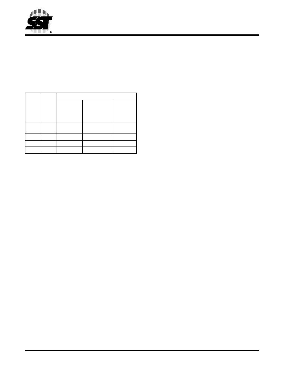
TABLE
3-2: SFCF Values Under Different Reset
Conditions
SC11
1. P = Programmed (Bit logic state = 0),
U = Unprogrammed (Bit logic state = 1)
State of SFCF[1:0] after:
Power-on
or
External
Reset
WDT Reset
or
Brown-out
Reset
Software
Reset
U (1)
00
(default)
x0
10
U (1)
P (0)
01
x1
11
P (0)
U (1)
10
P (0)
11
T3-2.0 1339
相关PDF资料 |
PDF描述 |
|---|---|
| SST89E58RD2-40-C-PIE | 8-BIT, FLASH, 40 MHz, MICROCONTROLLER, PDIP40 |
| SST89V516RD2-33-I-PIE | 8-BIT, FLASH, 33 MHz, MICROCONTROLLER, PDIP40 |
| SST89V54RD2-33-C-PIE | 8-BIT, FLASH, 33 MHz, MICROCONTROLLER, PDIP40 |
| SST89E516RD2-40-C-PIE | 8-BIT, FLASH, 40 MHz, MICROCONTROLLER, PDIP40 |
| ST16C1450CJ28-F | 1 CHANNEL(S), 1.5M bps, SERIAL COMM CONTROLLER, PQCC28 |
相关代理商/技术参数 |
参数描述 |
|---|---|
| SST89E54RD2A-40-C-NJE-ZZ131 | 制造商:Microchip Technology Inc 功能描述:4.5 TO 5.5V FLASHFLEX 8-BIT 8051 MICROCONTROLLER - Rail/Tube |
| SST89E54RD2A-40-C-TQJE | 功能描述:8位微控制器 -MCU 8-Bit 16K+8K Flash 40MHz 3/16-Bit Timer RoHS:否 制造商:Silicon Labs 核心:8051 处理器系列:C8051F39x 数据总线宽度:8 bit 最大时钟频率:50 MHz 程序存储器大小:16 KB 数据 RAM 大小:1 KB 片上 ADC:Yes 工作电源电压:1.8 V to 3.6 V 工作温度范围:- 40 C to + 105 C 封装 / 箱体:QFN-20 安装风格:SMD/SMT |
| SST89E54RD2A-40-C-TQJE-T | 功能描述:8位微控制器 -MCU 4.5-5.5V FL Flex 8B 8051 Microcontroller RoHS:否 制造商:Silicon Labs 核心:8051 处理器系列:C8051F39x 数据总线宽度:8 bit 最大时钟频率:50 MHz 程序存储器大小:16 KB 数据 RAM 大小:1 KB 片上 ADC:Yes 工作电源电压:1.8 V to 3.6 V 工作温度范围:- 40 C to + 105 C 封装 / 箱体:QFN-20 安装风格:SMD/SMT |
| SST89E54RD2RD | 制造商:SST 制造商全称:Silicon Storage Technology, Inc 功能描述:FlashFlex51 MCU |
| SST89E54RD2-RD | 制造商:SST 制造商全称:Silicon Storage Technology, Inc 功能描述:FlashFlex51 MCU |
发布紧急采购,3分钟左右您将得到回复。