- 您现在的位置:买卖IC网 > PDF目录98143 > ST10F296TR (STMICROELECTRONICS) 16-BIT, FLASH, 64 MHz, MICROCONTROLLER, PBGA208 PDF资料下载
参数资料
| 型号: | ST10F296TR |
| 厂商: | STMICROELECTRONICS |
| 元件分类: | 微控制器/微处理器 |
| 英文描述: | 16-BIT, FLASH, 64 MHz, MICROCONTROLLER, PBGA208 |
| 封装: | 23 X 23 MM, 1.96 MM HEIGHT, 1.27 MM PITCH, ROHS COMPLIANT, PLASTIC, BGA-208 |
| 文件页数: | 40/346页 |
| 文件大小: | 5607K |
| 代理商: | ST10F296TR |
第1页第2页第3页第4页第5页第6页第7页第8页第9页第10页第11页第12页第13页第14页第15页第16页第17页第18页第19页第20页第21页第22页第23页第24页第25页第26页第27页第28页第29页第30页第31页第32页第33页第34页第35页第36页第37页第38页第39页当前第40页第41页第42页第43页第44页第45页第46页第47页第48页第49页第50页第51页第52页第53页第54页第55页第56页第57页第58页第59页第60页第61页第62页第63页第64页第65页第66页第67页第68页第69页第70页第71页第72页第73页第74页第75页第76页第77页第78页第79页第80页第81页第82页第83页第84页第85页第86页第87页第88页第89页第90页第91页第92页第93页第94页第95页第96页第97页第98页第99页第100页第101页第102页第103页第104页第105页第106页第107页第108页第109页第110页第111页第112页第113页第114页第115页第116页第117页第118页第119页第120页第121页第122页第123页第124页第125页第126页第127页第128页第129页第130页第131页第132页第133页第134页第135页第136页第137页第138页第139页第140页第141页第142页第143页第144页第145页第146页第147页第148页第149页第150页第151页第152页第153页第154页第155页第156页第157页第158页第159页第160页第161页第162页第163页第164页第165页第166页第167页第168页第169页第170页第171页第172页第173页第174页第175页第176页第177页第178页第179页第180页第181页第182页第183页第184页第185页第186页第187页第188页第189页第190页第191页第192页第193页第194页第195页第196页第197页第198页第199页第200页第201页第202页第203页第204页第205页第206页第207页第208页第209页第210页第211页第212页第213页第214页第215页第216页第217页第218页第219页第220页第221页第222页第223页第224页第225页第226页第227页第228页第229页第230页第231页第232页第233页第234页第235页第236页第237页第238页第239页第240页第241页第242页第243页第244页第245页第246页第247页第248页第249页第250页第251页第252页第253页第254页第255页第256页第257页第258页第259页第260页第261页第262页第263页第264页第265页第266页第267页第268页第269页第270页第271页第272页第273页第274页第275页第276页第277页第278页第279页第280页第281页第282页第283页第284页第285页第286页第287页第288页第289页第290页第291页第292页第293页第294页第295页第296页第297页第298页第299页第300页第301页第302页第303页第304页第305页第306页第307页第308页第309页第310页第311页第312页第313页第314页第315页第316页第317页第318页第319页第320页第321页第322页第323页第324页第325页第326页第327页第328页第329页第330页第331页第332页第333页第334页第335页第336页第337页第338页第339页第340页第341页第342页第343页第344页第345页第346页
Parallel ports
ST10F296E
134/346
ODP2 register
13.4.2
Alternate functions of Port 2
All Port 2 lines (P2.15 to P2.0) can be configured as capture inputs or compare outputs
(CC15IO to CC0IO) for the CAPCOM1 unit.
When a Port 2 line is used as a capture input, the state of the input latch, which represents
the state of the port pin, is directed to the CAPCOM unit via the line ‘alternate pin data
input’. If an external capture trigger signal is used, the direction of the respective pin must be
set to input. If the direction is set to output, the state of the port output latch is read since the
pin represents the state of the output latch. This may trigger a capture event through
software by setting or clearing the port latch. Note that in the output configuration, no
external device may drive the pin, otherwise conflicts occur.
When a Port 2 line is used as a compare output (compare modes 1 and 3), the compare
event (or the timer overflow in compare mode 3) directly affects the port output latch. In
compare mode 1, when a valid compare match occurs, the state of the port output latch is
read by the CAPCOM control hardware via the line ‘alternate latch data input’. It is inverted
and written back to the latch via the line ‘alternate data output’. The port output latch is
clocked by the signal ‘compare trigger’ which is generated by the CAPCOM unit.
In compare mode 3, when a match occurs, the value 1 is written to the port output latch via
the line ‘alternate data output’. When an overflow of the corresponding timer occurs, a 0 is
written to the port output latch. In both cases, the output latch is clocked by the signal
‘compare trigger’. The direction of the pin should be set to output by the user, otherwise the
pin is in the high impedance state and does not reflect the state of the output latch.
As can be seen from the port structure (Figure 37), the user software always has free
access to the port pin even when it is used as a compare output. This is useful for setting up
the initial level of the pin when using compare mode 1 or the double-register mode. In these
modes, unlike in compare mode 3, the pin is not set to a specific value when a compare
match occurs. It is toggled instead.
When the user wants to write to the port pin at the same time a compare trigger tries to
clock the output latch, the write operation of the user software has priority. Each time a CPU
write access to the port output latch occurs, the input multiplexer of the port output latch is
switched to the line connected to the internal bus. The port output latch receives the value
from the internal bus and the hardware triggered change is lost.
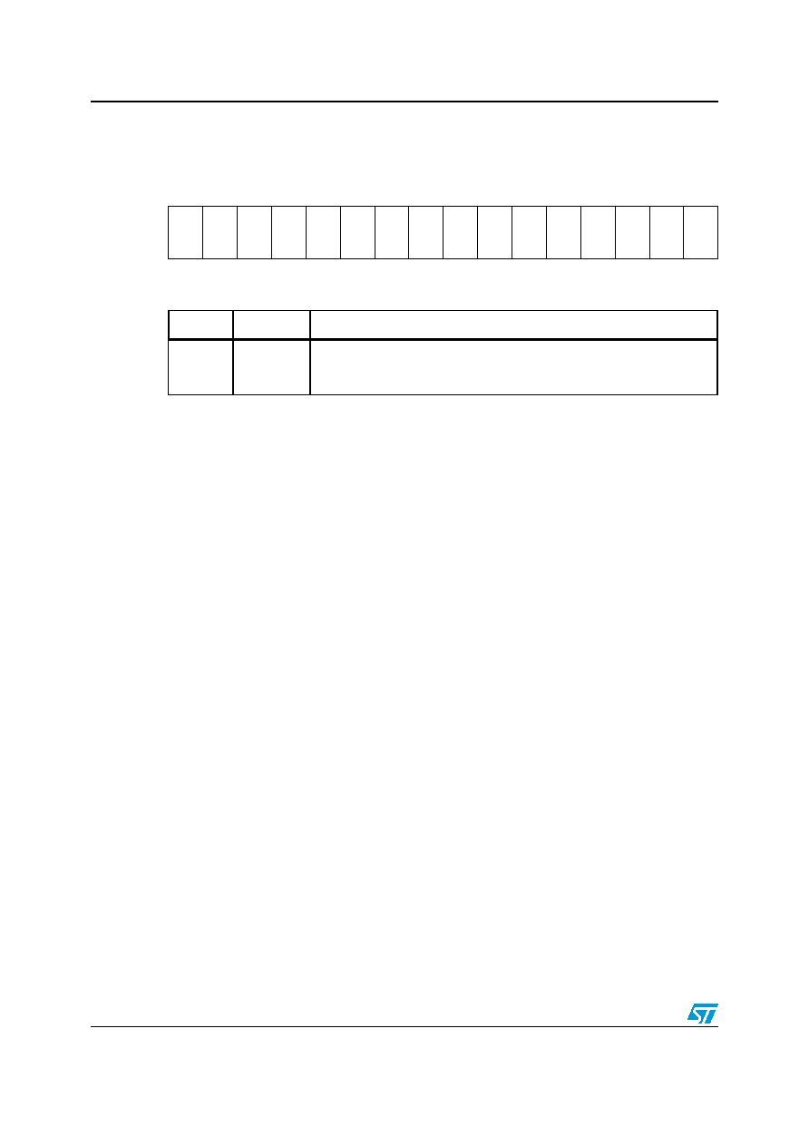
ODP2 (F1C2h/E1h)
ESFR
Reset value: 0000h
15
14
13
12
11
10
987
65432
10
OD
P2
.15
OD
P2
.14
OD
P2
.13
OD
P2
.12
OD
P2
.11
OD
P2
.10
OD
P2
.9
OD
P2
.8
OD
P2
.7
OD
P2
.6
OD
P2
.5
OD
P2
.4
OD
P2
.3
OD
P2
.2
OD
P2
.1
OD
P2
.0
RW
Table 73.
ODP2 register description
Bit
Bit name
Function
15-0
ODP2.y
Port open-drain control register ODP2 bit y
0: Port line P2.y output driver in push-pull mode
1: Port line P2.y output driver in open-drain mode
相关PDF资料 |
PDF描述 |
|---|---|
| ST10R172LT6 | 16-BIT, 50 MHz, MICROCONTROLLER, PQFP100 |
| ST10R272LT6 | 16-BIT, 50 MHz, MICROCONTROLLER, PQFP100 |
| ST16C452PSIJ68 | 2 CHANNEL(S), SERIAL COMM CONTROLLER, PQCC68 |
| ST16C452ATIJ68 | 2 CHANNEL(S), SERIAL COMM CONTROLLER, PQCC68 |
| ST16C654IQ64/TR | 4 CHANNEL(S), 1.5M bps, SERIAL COMM CONTROLLER, PQFP64 |
相关代理商/技术参数 |
参数描述 |
|---|---|
| ST10-IP-EE | 功能描述:电机驱动器 RoHS:否 制造商:Applied Motion 电机驱动类型:2035 Step 电源电压:12 V to 35 V 功率额定值:70 W 每转步距分辨率:200 to 400 框架大小 (NEMA): |
| ST10-IP-EE (5000-182) | 功能描述:电机驱动器 RoHS:否 制造商:Applied Motion 电机驱动类型:2035 Step 电源电压:12 V to 35 V 功率额定值:70 W 每转步距分辨率:200 to 400 框架大小 (NEMA): |
| ST10-IP-EN | 功能描述:电机驱动器 RoHS:否 制造商:Applied Motion 电机驱动类型:2035 Step 电源电压:12 V to 35 V 功率额定值:70 W 每转步距分辨率:200 to 400 框架大小 (NEMA): |
| ST10-IP-EN (5000-181) | 功能描述:电机驱动器 RoHS:否 制造商:Applied Motion 电机驱动类型:2035 Step 电源电压:12 V to 35 V 功率额定值:70 W 每转步距分辨率:200 to 400 框架大小 (NEMA): |
| ST10-PE | 制造商:Phoenix Contact 功能描述:TERMINAL ST 10-PE |
发布紧急采购,3分钟左右您将得到回复。