- 您现在的位置:买卖IC网 > PDF目录98144 > ST62P35BQ1/XXX (STMICROELECTRONICS) 8-BIT, MROM, 8 MHz, MICROCONTROLLER, PQFP52 PDF资料下载
参数资料
| 型号: | ST62P35BQ1/XXX |
| 厂商: | STMICROELECTRONICS |
| 元件分类: | 微控制器/微处理器 |
| 英文描述: | 8-BIT, MROM, 8 MHz, MICROCONTROLLER, PQFP52 |
| 封装: | PLASTIC, QFP-52 |
| 文件页数: | 49/82页 |
| 文件大小: | 617K |
| 代理商: | ST62P35BQ1/XXX |
第1页第2页第3页第4页第5页第6页第7页第8页第9页第10页第11页第12页第13页第14页第15页第16页第17页第18页第19页第20页第21页第22页第23页第24页第25页第26页第27页第28页第29页第30页第31页第32页第33页第34页第35页第36页第37页第38页第39页第40页第41页第42页第43页第44页第45页第46页第47页第48页当前第49页第50页第51页第52页第53页第54页第55页第56页第57页第58页第59页第60页第61页第62页第63页第64页第65页第66页第67页第68页第69页第70页第71页第72页第73页第74页第75页第76页第77页第78页第79页第80页第81页第82页
53/82
ST62T35B/E35B
4.4 A/D CONVERTER (ADC)
The A/D converter peripheral is an 8-bit analog to
digital converter with analog inputs as alternate
I/O functions (the number of which is device de-
pendent), offering 8-bit resolution with a selecta-
ble conversion time of 70us or 35
s (at an oscilla-
tor clock frequency of 8MHz).
The ADC converts the input voltage by a process
of successive approximations, using a clock fre-
quency derived from the oscillator with a division
factor of 12 or 6. After Reset, division by 12 is
used by default to insure compatibility with other
members of the ST62 MCU family. With an oscil-
lator clock frequency less than 1.2MHz, conver-
sion accuracy is decreased.
Selection of the input pin is done by configuring
the related I/O line as an analog input via the Op-
tion and Data registers (refer to I/O ports descrip-
tion for additional information). Only one I/O line
must be configured as an analog input at any time.
The user must avoid any situation in which more
than one I/O pin is selected as an analog input si-
multaneously, to avoid device malfunction.
The ADC uses two registers in the data space: the
ADC data conversion register, ADR, which stores
the conversion result, and the ADC control regis-
ter, ADCR, used to program the ADC functions.
A conversion is started by writing a “1” to the Start
bit (STA) in the ADC control register. This auto-
matically clears (resets to “0”) the End Of Conver-
sion Bit (EOC). When a conversion is complete,
the EOC bit is automatically set to “1”, in order to
flag that conversion is complete and that the data
in the ADC data conversion register is valid. Each
conversion has to be separately initiated by writing
to the STA bit.
The STA bit is continuously scanned so that, if the
user sets it to “1” while a previous conversion is in
progress, a new conversion is started before com-
pleting the previous one. The start bit (STA) is a
write only bit, any attempt to read it will show a log-
ical “0”.
The A/D converter features a maskable interrupt
associated with the end of conversion. The inter-
rupt request occurs when the EOC bit is set (i.e.
when a conversion is completed). The interrupt is
masked using the EAI (interrupt mask) bit in the
control register.
The power consumption of the device can be re-
duced by turning off the ADC peripheral. This is
done by setting the PDS bit in the ADC control
register to “0”. If PDS=“1”, the A/D is powered and
enabled for conversion. This bit must be set at
least one instruction before the beginning of the
conversion to allow stabilisation of the A/D con-
verter. This action is also needed before entering
WAIT mode, since the A/D comparator is not auto-
matically disabled in WAIT mode.
During Reset, any conversion in progress is
stopped, the control register is reset to 40h and
the ADC interrupt is masked (EAI=0).
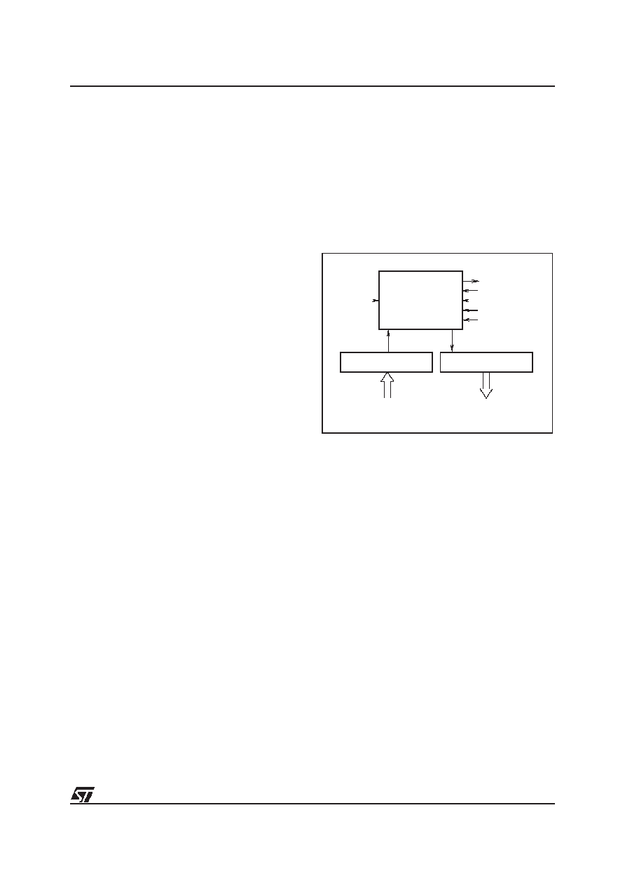
Figure 30. ADC Block Diagram
4.4.1 Application Notes
The A/D converter does not feature a sample and
hold circuit. The analog voltage to be measured
should therefore be stable during the entire con-
version cycle. Voltage variation should not exceed
±1/2 LSB for the optimum conversion accuracy. A
low pass filter may be used at the analog input
pins to reduce input voltage variation during con-
version.
When selected as an analog channel, the input pin
is internally connected to a capacitor Cad of typi-
cally 12pF. For maximum accuracy, this capacitor
must be fully charged at the beginning of conver-
sion. In the worst case, conversion starts one in-
struction (6.5
s) after the channel has been se-
lected. In worst case conditions, the impedance,
ASI, of the analog voltage source is calculated us-
ing the following formula:
6.5
s= 9 x C
ad xASI
(capacitor charged to over 99.9%), i.e. 30 k
in-
cluding a 50% guardband. ASI can be higher if
Cad has been charged for a longer period by add-
ing instructions before the start of conversion
(adding more than 26 CPU cycles is pointless).
CORE
CONTROL REGISTER
CONVERTER
VA00418
RESULT REGISTER
RESET
INTERRUPT
CLOCK
AV
AVDD
Ain
8
CORE
CONTROL SIGNALS
SS
8
52
相关PDF资料 |
PDF描述 |
|---|---|
| ST6235BQ1/XXX | 8-BIT, MROM, 8 MHz, MICROCONTROLLER, PQFP52 |
| ST62P45BQ6/XXX | 8-BIT, MROM, 8 MHz, MICROCONTROLLER, PQFP52 |
| ST62T03CM6E | 8-BIT, OTPROM, 8 MHz, MICROCONTROLLER, PDSO16 |
| ST62T10BM6 | 8-BIT, OTPROM, 8 MHz, MICROCONTROLLER, PDSO20 |
| ST62T25BB6 | 8-BIT, OTPROM, 8 MHz, MICROCONTROLLER, PDIP28 |
相关代理商/技术参数 |
参数描述 |
|---|---|
| ST62P52C | 制造商:STMicroelectronics 功能描述: |
| ST62P62CM6/MOMTR | 制造商:STMicroelectronics 功能描述: |
| ST62P62CM6/MPITR | 制造商:STMicroelectronics 功能描述: |
| ST62P62CM6/MSATR | 制造商:STMicroelectronics 功能描述: |
| ST62P62CN6/MMMTR | 制造商:STMicroelectronics 功能描述: |
发布紧急采购,3分钟左右您将得到回复。