- 您现在的位置:买卖IC网 > PDF目录195890 > ST72F324K4 64Mb EDO/FPM - OBSOLETE PDF资料下载
参数资料
| 型号: | ST72F324K4 |
| 英文描述: | 64Mb EDO/FPM - OBSOLETE |
| 中文描述: | 8位微控制器嵌套中断。闪光。 10位ADC。 4定时器。的SPI。 SCI接口 |
| 文件页数: | 130/161页 |
| 文件大小: | 2070K |
| 代理商: | ST72F324K4 |
第1页第2页第3页第4页第5页第6页第7页第8页第9页第10页第11页第12页第13页第14页第15页第16页第17页第18页第19页第20页第21页第22页第23页第24页第25页第26页第27页第28页第29页第30页第31页第32页第33页第34页第35页第36页第37页第38页第39页第40页第41页第42页第43页第44页第45页第46页第47页第48页第49页第50页第51页第52页第53页第54页第55页第56页第57页第58页第59页第60页第61页第62页第63页第64页第65页第66页第67页第68页第69页第70页第71页第72页第73页第74页第75页第76页第77页第78页第79页第80页第81页第82页第83页第84页第85页第86页第87页第88页第89页第90页第91页第92页第93页第94页第95页第96页第97页第98页第99页第100页第101页第102页第103页第104页第105页第106页第107页第108页第109页第110页第111页第112页第113页第114页第115页第116页第117页第118页第119页第120页第121页第122页第123页第124页第125页第126页第127页第128页第129页当前第130页第131页第132页第133页第134页第135页第136页第137页第138页第139页第140页第141页第142页第143页第144页第145页第146页第147页第148页第149页第150页第151页第152页第153页第154页第155页第156页第157页第158页第159页第160页第161页
ST72324
70/161
16-BIT TIMER (Cont’d)
10.3.3.6 Pulse Width Modulation Mode
Pulse Width Modulation (PWM) mode enables the
generation of a signal with a frequency and pulse
length determined by the value of the OC1R and
OC2R registers.
Pulse Width Modulation mode uses the complete
Output Compare 1 function plus the OC2R regis-
ter, and so this functionality can not be used when
PWM mode is activated.
In PWM mode, double buffering is implemented on
the output compare registers. Any new values writ-
ten in the OC1R and OC2R registers are taken
into account only at the end of the PWM period
(OC2) to avoid spikes on the PWM output pin
(OCMP1).
Procedure
To use pulse width modulation mode:
1. Load the OC2R register with the value corre-
sponding to the period of the signal using the
formula in the opposite column.
2. Load the OC1R register with the value corre-
sponding to the period of the pulse if (OLVL1=0
and OLVL2=1) using the formula in the oppo-
site column.
3. Select the following in the CR1 register:
– Using the OLVL1 bit, select the level to be ap-
plied to the OCMP1 pin after a successful
comparison with the OC1R register.
– Using the OLVL2 bit, select the level to be ap-
plied to the OCMP1 pin after a successful
comparison with the OC2R register.
4. Select the following in the CR2 register:
– Set OC1E bit: the OCMP1 pin is then dedicat-
ed to the output compare 1 function.
– Set the PWM bit.
– Select the timer clock (CC[1:0]) (see Table 15
If OLVL1=1 and OLVL2=0 the length of the posi-
tive pulse is the difference between the OC2R and
OC1R registers.
If OLVL1=OLVL2 a continuous signal will be seen
on the OCMP1 pin.
The OCiR register value required for a specific tim-
ing application can be calculated using the follow-
ing formula:
Where:
t
= Signal or pulse period (in seconds)
fCPU
= CPU clock frequency (in hertz)
PRESC = Timer prescaler factor (2, 4 or 8 depend-
ing on CC[1:0] bits, see Table 15)
If the timer clock is an external clock the formula is:
Where:
t
= Signal or pulse period (in seconds)
fEXT
= External timer clock frequency (in hertz)
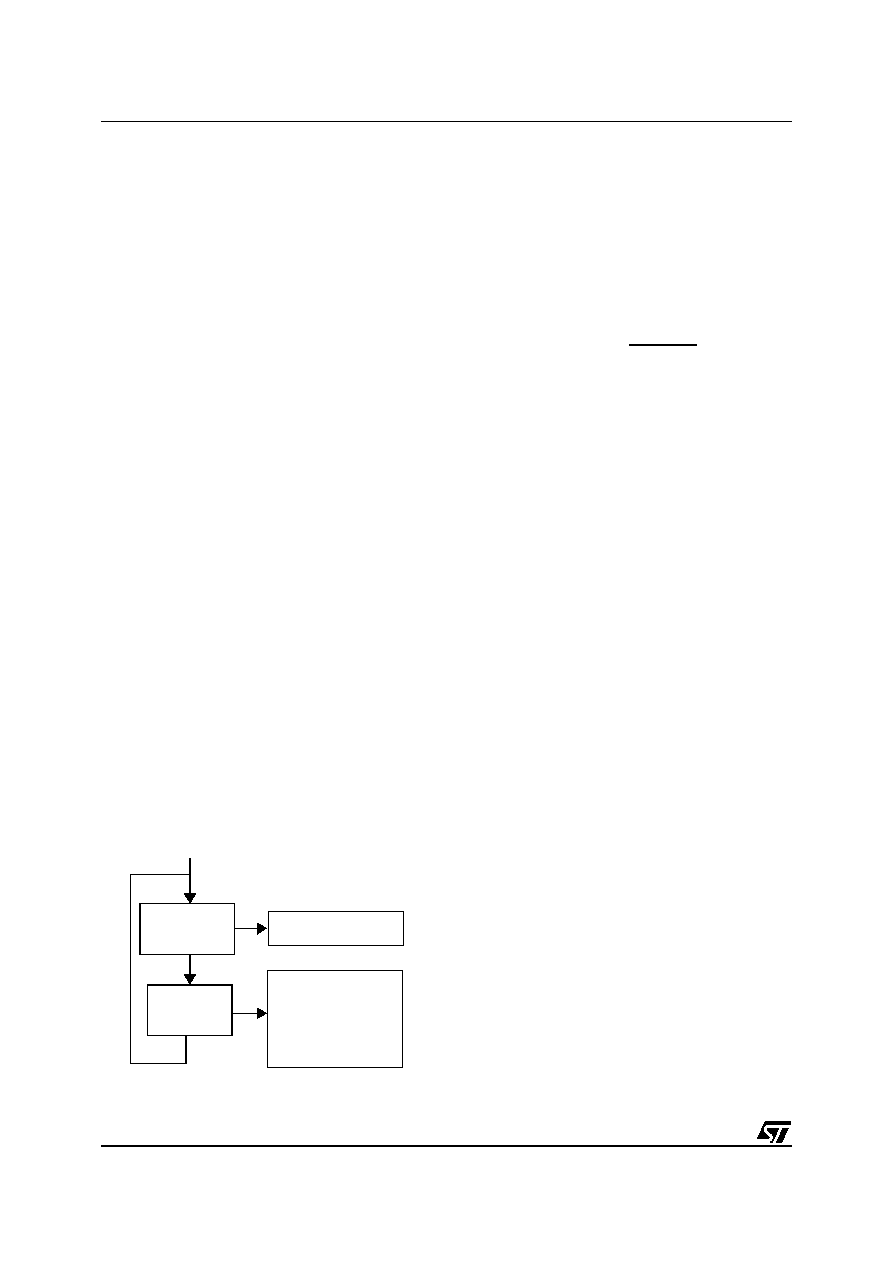
The Output Compare 2 event causes the counter
to be initialized to FFFCh (See Figure 46)
Notes:
1. After a write instruction to the OC
iHR register,
the output compare function is inhibited until the
OC
iLR register is also written.
2. The OCF1 and OCF2 bits cannot be set by
hardware in PWM mode therefore the Output
Compare interrupt is inhibited.
3. The ICF1 bit is set by hardware when the coun-
ter reaches the OC2R value and can produce a
timer interrupt if the ICIE bit is set and the I bit is
cleared.
4. In PWM mode the ICAP1 pin can not be used
to perform input capture because it is discon-
nected to the timer. The ICAP2 pin can be used
to perform input capture (ICF2 can be set and
IC2R can be loaded) but the user must take
care that the counter is reset each period and
ICF1 can also generates interrupt if ICIE is set.
5. When the Pulse Width Modulation (PWM) and
One Pulse Mode (OPM) bits are both set, the
PWM mode is the only active one.
6. The TAOC2HR, TAOC2LR registers in Timer A
are "write only". A read operation returns an
undefined value.
7. The ICAP2 registers (TAIC2HR, TAIC2LR) are
not available in Timer A. The ICF2 bit is forced by
hardware to 0.
Counter
OCMP1 = OLVL2
Counter
= OC2R
OCMP1 = OLVL1
When
= OC1R
Pulse Width Modulation cycle
Counter is reset
to FFFCh
ICF1 bit is set
OC
iR Value =
t * fCPU
PRESC
- 5
OC
iR =
t * fEXT -5
相关PDF资料 |
PDF描述 |
|---|---|
| ST72F324K6 | 64Mb EDO/FPM - OBSOLETE |
| ST72F611F1 | 64Mb EDO/FPM - OBSOLETE |
| ST72F611F1B1 | 64Mb EDO/FPM - OBSOLETE |
| ST72P621L4B1 | LOW SPEED USB 8-BIT MCU WITH 3 ENDPOINTS. FLASH OR ROM MEMORY. LVD. WDG. 10-BIT ADC. 2 TIMERS. SCI. SPI |
| ST72T213G1B3 | 8-BIT MCU WITH 4 TO 8K ROM/OTP/EPROM, 256 BYTES RAM, ADC, WDG, SPI AND 1 OR 2 TIMERS |
相关代理商/技术参数 |
参数描述 |
|---|---|
| ST72F324K4B6 | 功能描述:8位微控制器 -MCU 5V RANGE 8B MCU RoHS:否 制造商:Silicon Labs 核心:8051 处理器系列:C8051F39x 数据总线宽度:8 bit 最大时钟频率:50 MHz 程序存储器大小:16 KB 数据 RAM 大小:1 KB 片上 ADC:Yes 工作电源电压:1.8 V to 3.6 V 工作温度范围:- 40 C to + 105 C 封装 / 箱体:QFN-20 安装风格:SMD/SMT |
| ST72F324K4T6 | 功能描述:8位微控制器 -MCU Flash 16K SPI/SCI RoHS:否 制造商:Silicon Labs 核心:8051 处理器系列:C8051F39x 数据总线宽度:8 bit 最大时钟频率:50 MHz 程序存储器大小:16 KB 数据 RAM 大小:1 KB 片上 ADC:Yes 工作电源电压:1.8 V to 3.6 V 工作温度范围:- 40 C to + 105 C 封装 / 箱体:QFN-20 安装风格:SMD/SMT |
| ST72F324K4T6TR | 功能描述:8位微控制器 -MCU 5V RANGE 8B MCU RoHS:否 制造商:Silicon Labs 核心:8051 处理器系列:C8051F39x 数据总线宽度:8 bit 最大时钟频率:50 MHz 程序存储器大小:16 KB 数据 RAM 大小:1 KB 片上 ADC:Yes 工作电源电压:1.8 V to 3.6 V 工作温度范围:- 40 C to + 105 C 封装 / 箱体:QFN-20 安装风格:SMD/SMT |
| ST72F324K4TA | 功能描述:8位微控制器 -MCU Flask 16K SPI/SCI RoHS:否 制造商:Silicon Labs 核心:8051 处理器系列:C8051F39x 数据总线宽度:8 bit 最大时钟频率:50 MHz 程序存储器大小:16 KB 数据 RAM 大小:1 KB 片上 ADC:Yes 工作电源电压:1.8 V to 3.6 V 工作温度范围:- 40 C to + 105 C 封装 / 箱体:QFN-20 安装风格:SMD/SMT |
| ST72F324K4TA/TR | 功能描述:8位微控制器 -MCU AUTO 8BIT MICRO RoHS:否 制造商:Silicon Labs 核心:8051 处理器系列:C8051F39x 数据总线宽度:8 bit 最大时钟频率:50 MHz 程序存储器大小:16 KB 数据 RAM 大小:1 KB 片上 ADC:Yes 工作电源电压:1.8 V to 3.6 V 工作温度范围:- 40 C to + 105 C 封装 / 箱体:QFN-20 安装风格:SMD/SMT |
发布紧急采购,3分钟左右您将得到回复。