- 您现在的位置:买卖IC网 > PDF目录195890 > ST72F324K4 64Mb EDO/FPM - OBSOLETE PDF资料下载
参数资料
| 型号: | ST72F324K4 |
| 英文描述: | 64Mb EDO/FPM - OBSOLETE |
| 中文描述: | 8位微控制器嵌套中断。闪光。 10位ADC。 4定时器。的SPI。 SCI接口 |
| 文件页数: | 133/161页 |
| 文件大小: | 2070K |
| 代理商: | ST72F324K4 |
第1页第2页第3页第4页第5页第6页第7页第8页第9页第10页第11页第12页第13页第14页第15页第16页第17页第18页第19页第20页第21页第22页第23页第24页第25页第26页第27页第28页第29页第30页第31页第32页第33页第34页第35页第36页第37页第38页第39页第40页第41页第42页第43页第44页第45页第46页第47页第48页第49页第50页第51页第52页第53页第54页第55页第56页第57页第58页第59页第60页第61页第62页第63页第64页第65页第66页第67页第68页第69页第70页第71页第72页第73页第74页第75页第76页第77页第78页第79页第80页第81页第82页第83页第84页第85页第86页第87页第88页第89页第90页第91页第92页第93页第94页第95页第96页第97页第98页第99页第100页第101页第102页第103页第104页第105页第106页第107页第108页第109页第110页第111页第112页第113页第114页第115页第116页第117页第118页第119页第120页第121页第122页第123页第124页第125页第126页第127页第128页第129页第130页第131页第132页当前第133页第134页第135页第136页第137页第138页第139页第140页第141页第142页第143页第144页第145页第146页第147页第148页第149页第150页第151页第152页第153页第154页第155页第156页第157页第158页第159页第160页第161页
ST72324
73/161
16-BIT TIMER (Cont’d)
CONTROL REGISTER 2 (CR2)
Read/Write
Reset Value: 0000 0000 (00h)
Bit 7 = OC1E
Output Compare 1 Pin Enable.
This bit is used only to output the signal from the
timer on the OCMP1 pin (OLV1 in Output Com-
pare mode, both OLV1 and OLV2 in PWM and
one-pulse mode). Whatever the value of the OC1E
bit, the Output Compare 1 function of the timer re-
mains active.
0: OCMP1 pin alternate function disabled (I/O pin
free for general-purpose I/O).
1: OCMP1 pin alternate function enabled.
Bit 6 = OC2E
Output Compare 2 Pin Enable.
This bit is used only to output the signal from the
timer on the OCMP2 pin (OLV2 in Output Com-
pare mode). Whatever the value of the OC2E bit,
the Output Compare 2 function of the timer re-
mains active.
0: OCMP2 pin alternate function disabled (I/O pin
free for general-purpose I/O).
1: OCMP2 pin alternate function enabled.
Note: This bit is not available in Timer A. It must
be kept at its reset value.
Bit 5 = OPM
One Pulse Mode.
0: One Pulse Mode is not active.
1: One Pulse Mode is active, the ICAP1 pin can be
used to trigger one pulse on the OCMP1 pin; the
active transition is given by the IEDG1 bit. The
length of the generated pulse depends on the
contents of the OC1R register.
Bit 4 = PWM
Pulse Width Modulation.
0: PWM mode is not active.
1: PWM mode is active, the OCMP1 pin outputs a
programmable cyclic signal; the length of the
pulse depends on the value of OC1R register;
the period depends on the value of OC2R regis-
ter.
Bit 3, 2 = CC[1:0]
Clock Control.
The timer clock mode depends on these bits:
Table 15. Clock Control Bits
Note: If the external clock pin is not available, pro-
gramming the external clock configuration stops
the counter.
Bit 1 = IEDG2
Input Edge 2.
This bit determines which type of level transition
on the ICAP2 pin will trigger the capture.
0: A falling edge triggers the capture.
1: A rising edge triggers the capture.
Bit 0 = EXEDG
External Clock Edge.
This bit determines which type of level transition
on the external clock pin EXTCLK will trigger the
counter register.
0: A falling edge triggers the counter register.
1: A rising edge triggers the counter register.
70
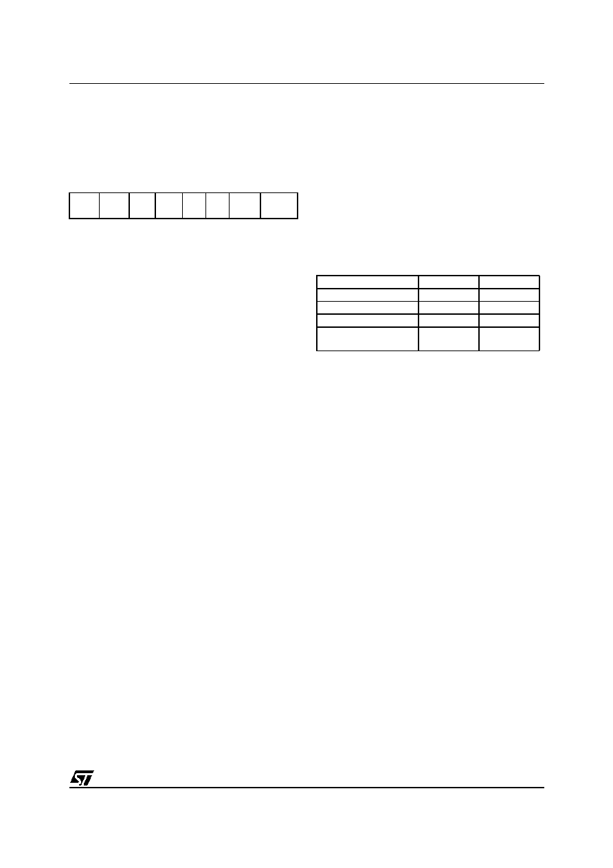
OC1E OC2E OPM PWM CC1 CC0 IEDG2 EXEDG
Timer Clock
CC1
CC0
fCPU / 4
0
fCPU / 2
0
1
fCPU / 8
1
0
External Clock (where
available)
11
相关PDF资料 |
PDF描述 |
|---|---|
| ST72F324K6 | 64Mb EDO/FPM - OBSOLETE |
| ST72F611F1 | 64Mb EDO/FPM - OBSOLETE |
| ST72F611F1B1 | 64Mb EDO/FPM - OBSOLETE |
| ST72P621L4B1 | LOW SPEED USB 8-BIT MCU WITH 3 ENDPOINTS. FLASH OR ROM MEMORY. LVD. WDG. 10-BIT ADC. 2 TIMERS. SCI. SPI |
| ST72T213G1B3 | 8-BIT MCU WITH 4 TO 8K ROM/OTP/EPROM, 256 BYTES RAM, ADC, WDG, SPI AND 1 OR 2 TIMERS |
相关代理商/技术参数 |
参数描述 |
|---|---|
| ST72F324K4B6 | 功能描述:8位微控制器 -MCU 5V RANGE 8B MCU RoHS:否 制造商:Silicon Labs 核心:8051 处理器系列:C8051F39x 数据总线宽度:8 bit 最大时钟频率:50 MHz 程序存储器大小:16 KB 数据 RAM 大小:1 KB 片上 ADC:Yes 工作电源电压:1.8 V to 3.6 V 工作温度范围:- 40 C to + 105 C 封装 / 箱体:QFN-20 安装风格:SMD/SMT |
| ST72F324K4T6 | 功能描述:8位微控制器 -MCU Flash 16K SPI/SCI RoHS:否 制造商:Silicon Labs 核心:8051 处理器系列:C8051F39x 数据总线宽度:8 bit 最大时钟频率:50 MHz 程序存储器大小:16 KB 数据 RAM 大小:1 KB 片上 ADC:Yes 工作电源电压:1.8 V to 3.6 V 工作温度范围:- 40 C to + 105 C 封装 / 箱体:QFN-20 安装风格:SMD/SMT |
| ST72F324K4T6TR | 功能描述:8位微控制器 -MCU 5V RANGE 8B MCU RoHS:否 制造商:Silicon Labs 核心:8051 处理器系列:C8051F39x 数据总线宽度:8 bit 最大时钟频率:50 MHz 程序存储器大小:16 KB 数据 RAM 大小:1 KB 片上 ADC:Yes 工作电源电压:1.8 V to 3.6 V 工作温度范围:- 40 C to + 105 C 封装 / 箱体:QFN-20 安装风格:SMD/SMT |
| ST72F324K4TA | 功能描述:8位微控制器 -MCU Flask 16K SPI/SCI RoHS:否 制造商:Silicon Labs 核心:8051 处理器系列:C8051F39x 数据总线宽度:8 bit 最大时钟频率:50 MHz 程序存储器大小:16 KB 数据 RAM 大小:1 KB 片上 ADC:Yes 工作电源电压:1.8 V to 3.6 V 工作温度范围:- 40 C to + 105 C 封装 / 箱体:QFN-20 安装风格:SMD/SMT |
| ST72F324K4TA/TR | 功能描述:8位微控制器 -MCU AUTO 8BIT MICRO RoHS:否 制造商:Silicon Labs 核心:8051 处理器系列:C8051F39x 数据总线宽度:8 bit 最大时钟频率:50 MHz 程序存储器大小:16 KB 数据 RAM 大小:1 KB 片上 ADC:Yes 工作电源电压:1.8 V to 3.6 V 工作温度范围:- 40 C to + 105 C 封装 / 箱体:QFN-20 安装风格:SMD/SMT |
发布紧急采购,3分钟左右您将得到回复。