- 您现在的位置:买卖IC网 > PDF目录195890 > ST72F324K4 64Mb EDO/FPM - OBSOLETE PDF资料下载
参数资料
| 型号: | ST72F324K4 |
| 英文描述: | 64Mb EDO/FPM - OBSOLETE |
| 中文描述: | 8位微控制器嵌套中断。闪光。 10位ADC。 4定时器。的SPI。 SCI接口 |
| 文件页数: | 66/161页 |
| 文件大小: | 2070K |
| 代理商: | ST72F324K4 |
第1页第2页第3页第4页第5页第6页第7页第8页第9页第10页第11页第12页第13页第14页第15页第16页第17页第18页第19页第20页第21页第22页第23页第24页第25页第26页第27页第28页第29页第30页第31页第32页第33页第34页第35页第36页第37页第38页第39页第40页第41页第42页第43页第44页第45页第46页第47页第48页第49页第50页第51页第52页第53页第54页第55页第56页第57页第58页第59页第60页第61页第62页第63页第64页第65页当前第66页第67页第68页第69页第70页第71页第72页第73页第74页第75页第76页第77页第78页第79页第80页第81页第82页第83页第84页第85页第86页第87页第88页第89页第90页第91页第92页第93页第94页第95页第96页第97页第98页第99页第100页第101页第102页第103页第104页第105页第106页第107页第108页第109页第110页第111页第112页第113页第114页第115页第116页第117页第118页第119页第120页第121页第122页第123页第124页第125页第126页第127页第128页第129页第130页第131页第132页第133页第134页第135页第136页第137页第138页第139页第140页第141页第142页第143页第144页第145页第146页第147页第148页第149页第150页第151页第152页第153页第154页第155页第156页第157页第158页第159页第160页第161页
ST72324
158/161
15.3 FLASH REV “X” and ALL ROM DEVICES
15.3.1 Read-out protection with LVD
The LVD is not supported if the read-out protection
is enabled.
15.3.2 External clock source with PLL
External clock source is not supported with the
PLL enabled.
15.3.3 I/O Port A and F Configuration
When using an external quartz crystal or ceramic
resonator, the fOSC2 clock may be disturbed be-
cause the device goes into reserved mode control-
led by Port A and F.
This happens with either one of the following con-
figurations:
PA3=0, PF4=1, PF1=0 while CSS and PLL op-
tions are both disabled and PF0 is toggling
PA3=0, PF4=1, PF1=0, PF0=1 while CSS or PLL
options are enabled
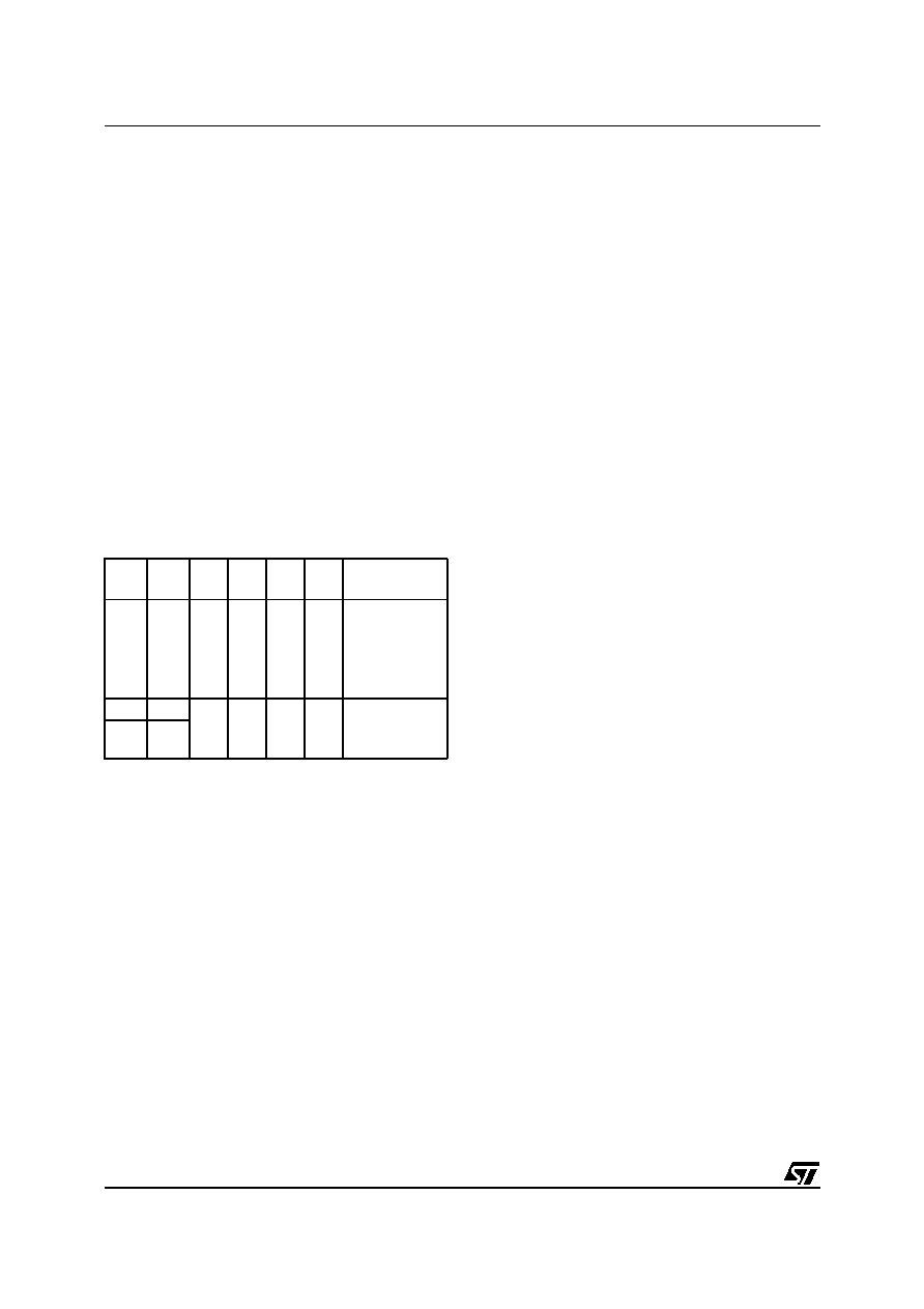
This is detailed in the following table:
As a consequence, for cycle-accurate operations,
these configurations are prohibited in either input
or output mode.
Workaround:
To avoid this occurring, it is recommended to con-
nect one of these pins to GND (PF4 or PF0) or
VDD (PA3 or PF1).
15.3.4 LVD Operation
Depending on the operating conditions, especially
the VDD ramp up speed and ambient temperature,
in some cases the LVD may not start. When this
occurs, the MCU may operate outside the guaran-
teed functional area (see datasheet Figure 76)
without being forced into reset state.
In this case, proper use of the watchdog may
make it possible to recover through a watchdog re-
set and allow normal operations to resume.
Consequently, the LVD function is not guaranteed
in the current silicon revision. For complete securi-
ty, an external reset circuit must be added.
15.4 ALL ROM DEVICES
15.4.1 AVD not supported
On some devices with a specific VDD ramp up
speed the AVD may not start. As a result it cannot
generate interrupts when VDD rises and falls.
15.4.2 Internal RC oscillator operation
Internal RC oscillator operation is not supported in
ROM devices.
CSS PLL PA3 PF4 PF1 PF0
Clock
Disturbance
OFF OFF
0
1
0
Tog
glin
g
Max. 2 clock
cycles lost at
each rising or
falling edge of
PF0
xON
01
Max. 1 clock
cycle lost out
of every 16
ON
x
相关PDF资料 |
PDF描述 |
|---|---|
| ST72F324K6 | 64Mb EDO/FPM - OBSOLETE |
| ST72F611F1 | 64Mb EDO/FPM - OBSOLETE |
| ST72F611F1B1 | 64Mb EDO/FPM - OBSOLETE |
| ST72P621L4B1 | LOW SPEED USB 8-BIT MCU WITH 3 ENDPOINTS. FLASH OR ROM MEMORY. LVD. WDG. 10-BIT ADC. 2 TIMERS. SCI. SPI |
| ST72T213G1B3 | 8-BIT MCU WITH 4 TO 8K ROM/OTP/EPROM, 256 BYTES RAM, ADC, WDG, SPI AND 1 OR 2 TIMERS |
相关代理商/技术参数 |
参数描述 |
|---|---|
| ST72F324K4B6 | 功能描述:8位微控制器 -MCU 5V RANGE 8B MCU RoHS:否 制造商:Silicon Labs 核心:8051 处理器系列:C8051F39x 数据总线宽度:8 bit 最大时钟频率:50 MHz 程序存储器大小:16 KB 数据 RAM 大小:1 KB 片上 ADC:Yes 工作电源电压:1.8 V to 3.6 V 工作温度范围:- 40 C to + 105 C 封装 / 箱体:QFN-20 安装风格:SMD/SMT |
| ST72F324K4T6 | 功能描述:8位微控制器 -MCU Flash 16K SPI/SCI RoHS:否 制造商:Silicon Labs 核心:8051 处理器系列:C8051F39x 数据总线宽度:8 bit 最大时钟频率:50 MHz 程序存储器大小:16 KB 数据 RAM 大小:1 KB 片上 ADC:Yes 工作电源电压:1.8 V to 3.6 V 工作温度范围:- 40 C to + 105 C 封装 / 箱体:QFN-20 安装风格:SMD/SMT |
| ST72F324K4T6TR | 功能描述:8位微控制器 -MCU 5V RANGE 8B MCU RoHS:否 制造商:Silicon Labs 核心:8051 处理器系列:C8051F39x 数据总线宽度:8 bit 最大时钟频率:50 MHz 程序存储器大小:16 KB 数据 RAM 大小:1 KB 片上 ADC:Yes 工作电源电压:1.8 V to 3.6 V 工作温度范围:- 40 C to + 105 C 封装 / 箱体:QFN-20 安装风格:SMD/SMT |
| ST72F324K4TA | 功能描述:8位微控制器 -MCU Flask 16K SPI/SCI RoHS:否 制造商:Silicon Labs 核心:8051 处理器系列:C8051F39x 数据总线宽度:8 bit 最大时钟频率:50 MHz 程序存储器大小:16 KB 数据 RAM 大小:1 KB 片上 ADC:Yes 工作电源电压:1.8 V to 3.6 V 工作温度范围:- 40 C to + 105 C 封装 / 箱体:QFN-20 安装风格:SMD/SMT |
| ST72F324K4TA/TR | 功能描述:8位微控制器 -MCU AUTO 8BIT MICRO RoHS:否 制造商:Silicon Labs 核心:8051 处理器系列:C8051F39x 数据总线宽度:8 bit 最大时钟频率:50 MHz 程序存储器大小:16 KB 数据 RAM 大小:1 KB 片上 ADC:Yes 工作电源电压:1.8 V to 3.6 V 工作温度范围:- 40 C to + 105 C 封装 / 箱体:QFN-20 安装风格:SMD/SMT |
发布紧急采购,3分钟左右您将得到回复。