- 您现在的位置:买卖IC网 > PDF目录69379 > ST7FMC1K2T6 (STMICROELECTRONICS) 8-BIT, FLASH, 8 MHz, MICROCONTROLLER, PQFP32 PDF资料下载
参数资料
| 型号: | ST7FMC1K2T6 |
| 厂商: | STMICROELECTRONICS |
| 元件分类: | 微控制器/微处理器 |
| 英文描述: | 8-BIT, FLASH, 8 MHz, MICROCONTROLLER, PQFP32 |
| 封装: | 7 X 7 MM, LQFP-32 |
| 文件页数: | 108/311页 |
| 文件大小: | 6511K |
| 代理商: | ST7FMC1K2T6 |
第1页第2页第3页第4页第5页第6页第7页第8页第9页第10页第11页第12页第13页第14页第15页第16页第17页第18页第19页第20页第21页第22页第23页第24页第25页第26页第27页第28页第29页第30页第31页第32页第33页第34页第35页第36页第37页第38页第39页第40页第41页第42页第43页第44页第45页第46页第47页第48页第49页第50页第51页第52页第53页第54页第55页第56页第57页第58页第59页第60页第61页第62页第63页第64页第65页第66页第67页第68页第69页第70页第71页第72页第73页第74页第75页第76页第77页第78页第79页第80页第81页第82页第83页第84页第85页第86页第87页第88页第89页第90页第91页第92页第93页第94页第95页第96页第97页第98页第99页第100页第101页第102页第103页第104页第105页第106页第107页当前第108页第109页第110页第111页第112页第113页第114页第115页第116页第117页第118页第119页第120页第121页第122页第123页第124页第125页第126页第127页第128页第129页第130页第131页第132页第133页第134页第135页第136页第137页第138页第139页第140页第141页第142页第143页第144页第145页第146页第147页第148页第149页第150页第151页第152页第153页第154页第155页第156页第157页第158页第159页第160页第161页第162页第163页第164页第165页第166页第167页第168页第169页第170页第171页第172页第173页第174页第175页第176页第177页第178页第179页第180页第181页第182页第183页第184页第185页第186页第187页第188页第189页第190页第191页第192页第193页第194页第195页第196页第197页第198页第199页第200页第201页第202页第203页第204页第205页第206页第207页第208页第209页第210页第211页第212页第213页第214页第215页第216页第217页第218页第219页第220页第221页第222页第223页第224页第225页第226页第227页第228页第229页第230页第231页第232页第233页第234页第235页第236页第237页第238页第239页第240页第241页第242页第243页第244页第245页第246页第247页第248页第249页第250页第251页第252页第253页第254页第255页第256页第257页第258页第259页第260页第261页第262页第263页第264页第265页第266页第267页第268页第269页第270页第271页第272页第273页第274页第275页第276页第277页第278页第279页第280页第281页第282页第283页第284页第285页第286页第287页第288页第289页第290页第291页第292页第293页第294页第295页第296页第297页第298页第299页第300页第301页第302页第303页第304页第305页第306页第307页第308页第309页第310页第311页
ST7MC1/ST7MC2
196/308
MOTOR CONTROLLER (Cont’d)
If the PCN bit is reset, one of the three PWM sig-
nals (the one set by the compare U register pair) or
the output of the measurement window generator
(depending on if the driving mode is voltage or cur-
rent) is used to provide six-step signals through
the PWM manager (to drive a PM BLDC motor for
instance).
In that case, DTE behaves like a standard bit (with
multiple write capability). When the deadtime gen-
erator is enabled (bit DTE=1), some restrictions
are applied, summarized in Table 53:
■ Channels
are
now
grouped
by
pairs:
Channel[0:1], Channel[2:3], Channel[4:5]; a
deadtime generator is allocated to each of these
pairs (see cautions below);
■ The input signal of the deadtime generator is the
active output of the PWM manager for the
corresponding channel. For instance, if we
consider the Channel[0:1] pair, it may be either
Channel0 or Channel1.
■ When both channels of a pair are inactive, the
corresponding outputs will also stay inactive
(this is mandatory to allow BEMF zero-crossing
detection).
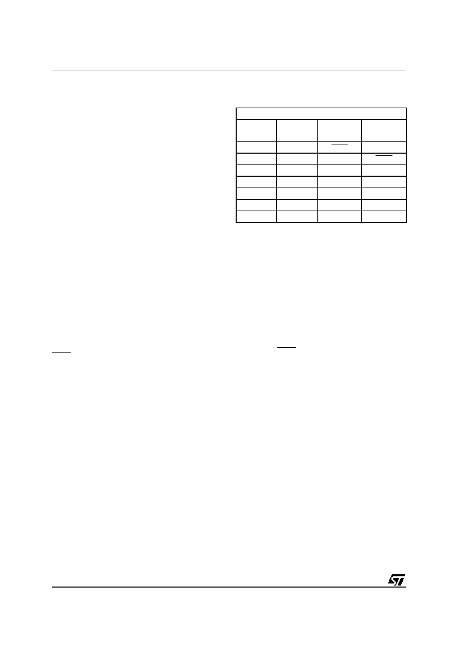
Table 53 summarizes the functionality of the dead-
time generator when the PCN bit is reset. 1(pwm*)
means that the corresponding channel is active (1
in the corresponding bit in the MPHST register),
and a PWM signal is applied on it (using the MPAR
register and the OS[2:0] bits in MCRB register).
PWM represents the complementary signals (al-
though the duty cycle is slightly different due to
deadtime insertion). 0 means that the channel is
inactive and 1 means that the channel is active
and a logic level 1 is applied on it (no PWM signal).
Table 53. Dead Time generator outputs
* PWM generation enabled
Warning: Grouping channels by pairs imposes the
external connections between the MCO outputs
and power devices; the user must therefore pay at-
tention to respect the “recommended schematics”
described in Figure 123. on page 227 and Figure
Note: As soon as the channels are grouped in
pairs, special care has to be taken in configuring
the MPAR register for a PM BLDC drive. If both
channels of the same pair are both labelled “high”
for example and if the PWM is applied on high
channels, the active MCO output x (OOx=1 bit in
the MPHST register) outputs PWM and the paired
MCO output x+1 (OOx+1bit in the MPHST regis-
ter) outputs PWM and vice versa.
Caution: When PCN=0 and a complementary
PWM is applied (DTE=1) on one channel of a pair,
if both channels are active, this corresponds in
output to both channels OFF. This is for security
purpose to avoid cross-conduction.
Caution: To clear the DTE bit from reset state of
MDTG register (FFh), the PCN bit must be cleared
before.
PCN = 0; DTE =1; x= 0, 2, 4
On/Off x
(OOx bit)
On/Off x+1
(OOx+1 bit)
MCOx output
MCOx+1
output
01 (pwm*)
PWM
1 (pwm*)
0
PWM
11 (pwm*)
0
1 (pwm*)
1
0
10
1
0
01
0
1
00
0
1
相关PDF资料 |
PDF描述 |
|---|---|
| ST7MC2S4T6/XXX | 8-BIT, FLASH, 8 MHz, MICROCONTROLLER, PQFP44 |
| ST7FMC2N6B6 | 8-BIT, FLASH, 8 MHz, MICROCONTROLLER, PDIP56 |
| ST7FMC2S6T6 | 8-BIT, FLASH, 8 MHz, MICROCONTROLLER, PQFP44 |
| ST7PMC2M9T6/XXX | 8-BIT, FLASH, 8 MHz, MICROCONTROLLER, PQFP80 |
| ST7PMC2R6T6/XXX | 8-BIT, FLASH, 8 MHz, MICROCONTROLLER, PQFP64 |
相关代理商/技术参数 |
参数描述 |
|---|---|
| ST7FMC1K2T6/TR | 功能描述:8位微控制器 -MCU 8B MCU WITH NESTED INTERRUPTS RoHS:否 制造商:Silicon Labs 核心:8051 处理器系列:C8051F39x 数据总线宽度:8 bit 最大时钟频率:50 MHz 程序存储器大小:16 KB 数据 RAM 大小:1 KB 片上 ADC:Yes 工作电源电压:1.8 V to 3.6 V 工作温度范围:- 40 C to + 105 C 封装 / 箱体:QFN-20 安装风格:SMD/SMT |
| ST7FMC1K2TC | 制造商:STMicroelectronics 功能描述: |
| ST7FMC1K2TCE | 功能描述:插座和适配器 MCU TQFP32 7x7 RoHS:否 制造商:Silicon Labs 产品:Adapter 用于:EM35x |
| ST7FMC1K4B3 | 制造商:STMICROELECTRONICS 制造商全称:STMicroelectronics 功能描述:8-bit MCU with nested interrupts, Flash, 10-bit ADC, brushless motor control, five timers, SPI, LINSCI? |
| ST7FMC1K4B6 | 制造商:STMICROELECTRONICS 制造商全称:STMicroelectronics 功能描述:8-bit MCU with nested interrupts, Flash, 10-bit ADC, brushless motor control, five timers, SPI, LINSCI? |
发布紧急采购,3分钟左右您将得到回复。