- 您现在的位置:买卖IC网 > PDF目录69379 > ST7FMC1K2T6 (STMICROELECTRONICS) 8-BIT, FLASH, 8 MHz, MICROCONTROLLER, PQFP32 PDF资料下载
参数资料
| 型号: | ST7FMC1K2T6 |
| 厂商: | STMICROELECTRONICS |
| 元件分类: | 微控制器/微处理器 |
| 英文描述: | 8-BIT, FLASH, 8 MHz, MICROCONTROLLER, PQFP32 |
| 封装: | 7 X 7 MM, LQFP-32 |
| 文件页数: | 123/311页 |
| 文件大小: | 6511K |
| 代理商: | ST7FMC1K2T6 |
第1页第2页第3页第4页第5页第6页第7页第8页第9页第10页第11页第12页第13页第14页第15页第16页第17页第18页第19页第20页第21页第22页第23页第24页第25页第26页第27页第28页第29页第30页第31页第32页第33页第34页第35页第36页第37页第38页第39页第40页第41页第42页第43页第44页第45页第46页第47页第48页第49页第50页第51页第52页第53页第54页第55页第56页第57页第58页第59页第60页第61页第62页第63页第64页第65页第66页第67页第68页第69页第70页第71页第72页第73页第74页第75页第76页第77页第78页第79页第80页第81页第82页第83页第84页第85页第86页第87页第88页第89页第90页第91页第92页第93页第94页第95页第96页第97页第98页第99页第100页第101页第102页第103页第104页第105页第106页第107页第108页第109页第110页第111页第112页第113页第114页第115页第116页第117页第118页第119页第120页第121页第122页当前第123页第124页第125页第126页第127页第128页第129页第130页第131页第132页第133页第134页第135页第136页第137页第138页第139页第140页第141页第142页第143页第144页第145页第146页第147页第148页第149页第150页第151页第152页第153页第154页第155页第156页第157页第158页第159页第160页第161页第162页第163页第164页第165页第166页第167页第168页第169页第170页第171页第172页第173页第174页第175页第176页第177页第178页第179页第180页第181页第182页第183页第184页第185页第186页第187页第188页第189页第190页第191页第192页第193页第194页第195页第196页第197页第198页第199页第200页第201页第202页第203页第204页第205页第206页第207页第208页第209页第210页第211页第212页第213页第214页第215页第216页第217页第218页第219页第220页第221页第222页第223页第224页第225页第226页第227页第228页第229页第230页第231页第232页第233页第234页第235页第236页第237页第238页第239页第240页第241页第242页第243页第244页第245页第246页第247页第248页第249页第250页第251页第252页第253页第254页第255页第256页第257页第258页第259页第260页第261页第262页第263页第264页第265页第266页第267页第268页第269页第270页第271页第272页第273页第274页第275页第276页第277页第278页第279页第280页第281页第282页第283页第284页第285页第286页第287页第288页第289页第290页第291页第292页第293页第294页第295页第296页第297页第298页第299页第300页第301页第302页第303页第304页第305页第306页第307页第308页第309页第310页第311页
ST7MC1/ST7MC2
209/308
MOTOR CONTROLLER (Cont’d)
CONTROL REGISTER A (MCRA)
Read/Write
Reset Value: 0000 0000 (00h)
Bit 7 = MOE: Output Enable bit.
0: Outputs disabled
1: Outputs enabled
Notes:
– The reset state is either high impedance, high or
low state depending on the corresponding option
bit.
– When the MOE bit in the MCRA register is reset
(MCOx outputs in reset state), and the SR bit in
the MCRA register is reset (sensorless mode)
and the SPLG bit in the MCRC register is reset
(sampling at PWM frequency) then, depending
on the state of the ZSV bit in the MSCR register,
Z event sampling can run or be stopped (and D
event is sampled).
Bit 6 = CKE: Clock Enable Bit.
0: Motor Control peripheral Clocks disabled
1: Motor Control peripheral Clocks enabled
Note: Clocks disabled means that all peripheral in-
ternal clocks (Delay manager, internal sampling
clock, PWM generator) are disabled. Therefore,
the peripheral can no longer detect events and the
preload registers do not operate.
When Clocks are disabled, write accesses are al-
lowed, so for example, MTIM counter register can
be reset by software.
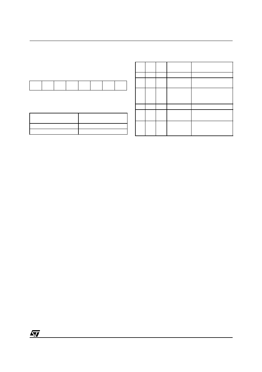
Table 56. Output configuration summary
Note 1: “Peripheral frozen” configuration is not
recommended, as the peripheral may be stopped
in a unknown state (depending on PWM generator
outputs,etc.). It is better practice to exit from run
mode by first setting output state (by toggling ei-
ther MOE or DAC bits) and then to disabling the
clock if needed.
Note 2: In Direct Access Mode (DAC=1), when
CKE=0 (Peripheral Clock disabled) only logical
level can be applied on the MCOx outputs when
they are enabled whereas when CKE=1 (Peripher-
al Clock enabled), a PWM signal can be applied
on them. Refer to Table 74, “DeadTime generator
Note 3: When clocks are disabled (CKE bit reset)
while outputs are enabled (MOE bit set), the ef-
fects on the MCOx outputs where PWM signal is
applied depend on the running mode selected:
– in voltage mode (VOC1 bit=0), the MCOx out-
puts where PWM signal is applied stay at level 1.
– in current mode (VOC1 bit=1), the MCOx outputs
where PWM signal is applied are put to level 0.
In all cases, MCOx outputs where a level 1 was
applied before disabling the clocks stay at level 1.
That is why it is recommended to disable the
MCOx outputs (reset MOE bit) before disabling the
clocks. This will put all the MCOx outputs under re-
set state defined by the corresponding option bit.
76
54
32
10
MOE
CKE
SR
DAC
V0C1
SWA
PZ
DCB
MOE bit
MCO[5:0] Output pin
State
0
Reset state
1
Output enabled
CKE
bit
MOE
bit
DAC
bit
Peripheral
Clock
Effect on MCOx
Output
0
x
Disabled
Reset state
0
1
0
Disabled
Peripheral frozen (see
note 1 below)
0
1
Disabled
Direct access via
MPHST
(only logical level)
1
0
x
Enabled
Reset state
1
0
Enabled
Standard
running mode.
1
Enabled
Direct access via
MPHST (PWM can be
applied)
1
相关PDF资料 |
PDF描述 |
|---|---|
| ST7MC2S4T6/XXX | 8-BIT, FLASH, 8 MHz, MICROCONTROLLER, PQFP44 |
| ST7FMC2N6B6 | 8-BIT, FLASH, 8 MHz, MICROCONTROLLER, PDIP56 |
| ST7FMC2S6T6 | 8-BIT, FLASH, 8 MHz, MICROCONTROLLER, PQFP44 |
| ST7PMC2M9T6/XXX | 8-BIT, FLASH, 8 MHz, MICROCONTROLLER, PQFP80 |
| ST7PMC2R6T6/XXX | 8-BIT, FLASH, 8 MHz, MICROCONTROLLER, PQFP64 |
相关代理商/技术参数 |
参数描述 |
|---|---|
| ST7FMC1K2T6/TR | 功能描述:8位微控制器 -MCU 8B MCU WITH NESTED INTERRUPTS RoHS:否 制造商:Silicon Labs 核心:8051 处理器系列:C8051F39x 数据总线宽度:8 bit 最大时钟频率:50 MHz 程序存储器大小:16 KB 数据 RAM 大小:1 KB 片上 ADC:Yes 工作电源电压:1.8 V to 3.6 V 工作温度范围:- 40 C to + 105 C 封装 / 箱体:QFN-20 安装风格:SMD/SMT |
| ST7FMC1K2TC | 制造商:STMicroelectronics 功能描述: |
| ST7FMC1K2TCE | 功能描述:插座和适配器 MCU TQFP32 7x7 RoHS:否 制造商:Silicon Labs 产品:Adapter 用于:EM35x |
| ST7FMC1K4B3 | 制造商:STMICROELECTRONICS 制造商全称:STMicroelectronics 功能描述:8-bit MCU with nested interrupts, Flash, 10-bit ADC, brushless motor control, five timers, SPI, LINSCI? |
| ST7FMC1K4B6 | 制造商:STMICROELECTRONICS 制造商全称:STMicroelectronics 功能描述:8-bit MCU with nested interrupts, Flash, 10-bit ADC, brushless motor control, five timers, SPI, LINSCI? |
发布紧急采购,3分钟左右您将得到回复。