- 您现在的位置:买卖IC网 > PDF目录98146 > ST90158P9C6 (STMICROELECTRONICS) 16-BIT, MROM, 16 MHz, MICROCONTROLLER, PQCC84 PDF资料下载
参数资料
| 型号: | ST90158P9C6 |
| 厂商: | STMICROELECTRONICS |
| 元件分类: | 微控制器/微处理器 |
| 英文描述: | 16-BIT, MROM, 16 MHz, MICROCONTROLLER, PQCC84 |
| 封装: | PLASTIC, LCC-84 |
| 文件页数: | 70/189页 |
| 文件大小: | 3326K |
| 代理商: | ST90158P9C6 |
第1页第2页第3页第4页第5页第6页第7页第8页第9页第10页第11页第12页第13页第14页第15页第16页第17页第18页第19页第20页第21页第22页第23页第24页第25页第26页第27页第28页第29页第30页第31页第32页第33页第34页第35页第36页第37页第38页第39页第40页第41页第42页第43页第44页第45页第46页第47页第48页第49页第50页第51页第52页第53页第54页第55页第56页第57页第58页第59页第60页第61页第62页第63页第64页第65页第66页第67页第68页第69页当前第70页第71页第72页第73页第74页第75页第76页第77页第78页第79页第80页第81页第82页第83页第84页第85页第86页第87页第88页第89页第90页第91页第92页第93页第94页第95页第96页第97页第98页第99页第100页第101页第102页第103页第104页第105页第106页第107页第108页第109页第110页第111页第112页第113页第114页第115页第116页第117页第118页第119页第120页第121页第122页第123页第124页第125页第126页第127页第128页第129页第130页第131页第132页第133页第134页第135页第136页第137页第138页第139页第140页第141页第142页第143页第144页第145页第146页第147页第148页第149页第150页第151页第152页第153页第154页第155页第156页第157页第158页第159页第160页第161页第162页第163页第164页第165页第166页第167页第168页第169页第170页第171页第172页第173页第174页第175页第176页第177页第178页第179页第180页第181页第182页第183页第184页第185页第186页第187页第188页第189页
161/189
SERIAL COMMUNICATIONS INTERFACE (SCI)
REGISTER DESCRIPTION (Cont’d)
Bit 0 = STPEN:
Stick Parity Enable.
0: The transmitter and the receiver will follow the
parity of even parity bit EP in the CHCR register.
1: The transmitter and the receiver will use the op-
posite parity type selected by the even parity bit
EP in the CHCR register.
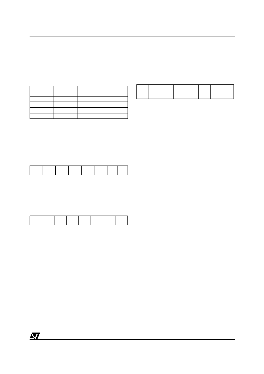
BAUD RATE GENERATOR HIGH REGISTER
(BRGHR)
R252 - Read/Write
Reset value: undefined
BAUD RATE GENERATOR LOW REGISTER
(BRGLR)
R253 - Read/Write
Reset value: undefined
Bit 15:0 =
Baud Rate Generator MSB and LSB.
The Baud Rate generator is a programmable di-
vide by “N” counter which can be used to generate
the clocks for the transmitter and/or receiver. This
counter divides the clock input by the value in the
Baud Rate Generator Register. The minimum
baud rate divisor is 2 and the maximum divisor is
216-1. After initialization of the baud rate genera-
tor, the divisor value is immediately loaded into the
counter. This prevents potentially long random
counts on the initial load. If set to 0 or 1, the Baud
Rate Generator is stopped.
SYNCHRONOUS INPUT CONTROL (SICR)
R254 - Read/Write
Reset value: 0000 0011 (03h)
Bit 7 = SMEN:
Synchronous Mode Enable.
0: Disable all features relating to Synchronous
mode (the contents of SICR and SOCR are ig-
nored).
1: Select Synchronous mode with its programmed
I/O configuration.
Bit 6 = INPL:
SIN Input Polarity.
0: Polarity not inverted.
1: Polarity inverted.
Note: INPL only affects received data. In Auto-
Echo mode SOUT = SIN even if INPL is set. In
Loop-Back mode the state of the INPL bit is irrele-
vant.
Bit 5 = XCKPL:
Receiver Clock Polarity.
0: RXCLK is active on the rising edge.
1: RXCLK is active on the falling edge.
Note: XCKPL only affects the receiver clock. In
Auto-Echo mode CLKOUT = RXCLK independ-
ently of the XCKPL status. In Loop-Back the state
of the XCKPL bit is irrelevant.
Bit 4 = DCDEN:
DCD Input Enable.
0: Disable hardware synchronization.
1: Enable hardware synchronization.
Note: When DCDEN is set, RXCLK drives the re-
ceiver section only during the active level of the
DCD input (DCD works as a gate on RXCLK, in-
forming the MCU that a transmitting device is
sending a synchronous frame to it).
Bit 3 = DCDPL:
DCD Input Polarity.
0: The DCD input is active when LOW.
1: The DCD input is active when HIGH.
Note: DCDPL only affects the gating activity of the
receiver clock. In Auto-Echo mode RTS = DCD in-
dependently of DCDPL. In Loop-Back mode, the
state of DCDPL is irrelevant.
EP
SPEN
Parity (Transmitter &
Receiver)
0 (odd)
0
Odd
1 (even)
0
Even
0 (odd)
1
Even
1 (even)
1
Odd
15
8
BG15
BG14
BG13
BG12
BG11
BG10
BG9
BG8
70
BG7
BG6
BG5
BG4
BG3
BG2
BG1
BG0
70
SMEN
INPL
XCKPL
DCDE
N
DCDP
L
INPEN
X
9
相关PDF资料 |
PDF描述 |
|---|---|
| ST90E28L1/ES | 16-BIT, UVPROM, 24 MHz, MICROCONTROLLER, CQCC44 |
| ST90E30D1/ES | 16-BIT, UVPROM, 24 MHz, MICROCONTROLLER, CDIP56 |
| ST90E30L1/ES | 16-BIT, UVPROM, 24 MHz, MICROCONTROLLER, CQCC68 |
| ST90T30B6 | 16-BIT, OTPROM, 24 MHz, MICROCONTROLLER, PDIP56 |
| ST90R40C1 | 16-BIT, 24 MHz, MICROCONTROLLER, PQCC68 |
相关代理商/技术参数 |
参数描述 |
|---|---|
| ST90158-ST90135 | 制造商:STMICROELECTRONICS 制造商全称:STMicroelectronics 功能描述:8/16-BIT MCU FAMILY WITH UP TO 64K ROM/OTP/EPROM AND UP TO 2K RAM |
| ST9016 | 制造商:SEMTECH_ELEC 制造商全称:SEMTECH ELECTRONICS LTD. 功能描述:NPN Silicon Epitaxial Planar Transistor |
| ST9018 | 制造商:SEMTECH_ELEC 制造商全称:SEMTECH ELECTRONICS LTD. 功能描述:NPN Silicon Epitaxial Planar Transistor |
| ST901T | 功能描述:达林顿晶体管 NPN Power Darlington RoHS:否 制造商:Texas Instruments 配置:Octal 晶体管极性:NPN 集电极—发射极最大电压 VCEO:50 V 发射极 - 基极电压 VEBO: 集电极—基极电压 VCBO: 最大直流电集电极电流:0.5 A 最大集电极截止电流: 功率耗散: 最大工作温度:+ 150 C 安装风格:SMD/SMT 封装 / 箱体:SOIC-18 封装:Reel |
| ST901T_05 | 制造商:STMICROELECTRONICS 制造商全称:STMicroelectronics 功能描述:HIGH VOLTAGE IGNITION COIL DRIVER NPN POWER TRANSISTOR |
发布紧急采购,3分钟左右您将得到回复。