参数资料
| 型号: | T89C51CC01UA-SLSIM |
| 厂商: | Atmel |
| 文件页数: | 102/123页 |
| 文件大小: | 0K |
| 描述: | IC 8051 MCU FLASH 32K 44PLCC |
| 标准包装: | 27 |
| 系列: | AT89C CAN |
| 核心处理器: | 8051 |
| 芯体尺寸: | 8-位 |
| 速度: | 40MHz |
| 连通性: | CAN,UART/USART |
| 外围设备: | POR,PWM,WDT |
| 输入/输出数: | 32 |
| 程序存储器容量: | 32KB(32K x 8) |
| 程序存储器类型: | 闪存 |
| EEPROM 大小: | 2K x 8 |
| RAM 容量: | 1.25K x 8 |
| 电压 - 电源 (Vcc/Vdd): | 3 V ~ 5.5 V |
| 数据转换器: | A/D 8x10b |
| 振荡器型: | 外部 |
| 工作温度: | -40°C ~ 85°C |
| 封装/外壳: | 44-LCC(J 形引线) |
| 包装: | 管件 |
| 配用: | AT89STK-06-ND - KIT DEMOBOARD 8051 MCU W/CAN |
| 其它名称: | T89C51CC01UASLSIM |
第1页第2页第3页第4页第5页第6页第7页第8页第9页第10页第11页第12页第13页第14页第15页第16页第17页第18页第19页第20页第21页第22页第23页第24页第25页第26页第27页第28页第29页第30页第31页第32页第33页第34页第35页第36页第37页第38页第39页第40页第41页第42页第43页第44页第45页第46页第47页第48页第49页第50页第51页第52页第53页第54页第55页第56页第57页第58页第59页第60页第61页第62页第63页第64页第65页第66页第67页第68页第69页第70页第71页第72页第73页第74页第75页第76页第77页第78页第79页第80页第81页第82页第83页第84页第85页第86页第87页第88页第89页第90页第91页第92页第93页第94页第95页第96页第97页第98页第99页第100页第101页当前第102页第103页第104页第105页第106页第107页第108页第109页第110页第111页第112页第113页第114页第115页第116页第117页第118页第119页第120页第121页第122页第123页
4
A/T89C51CC01
4129N–CAN–03/08
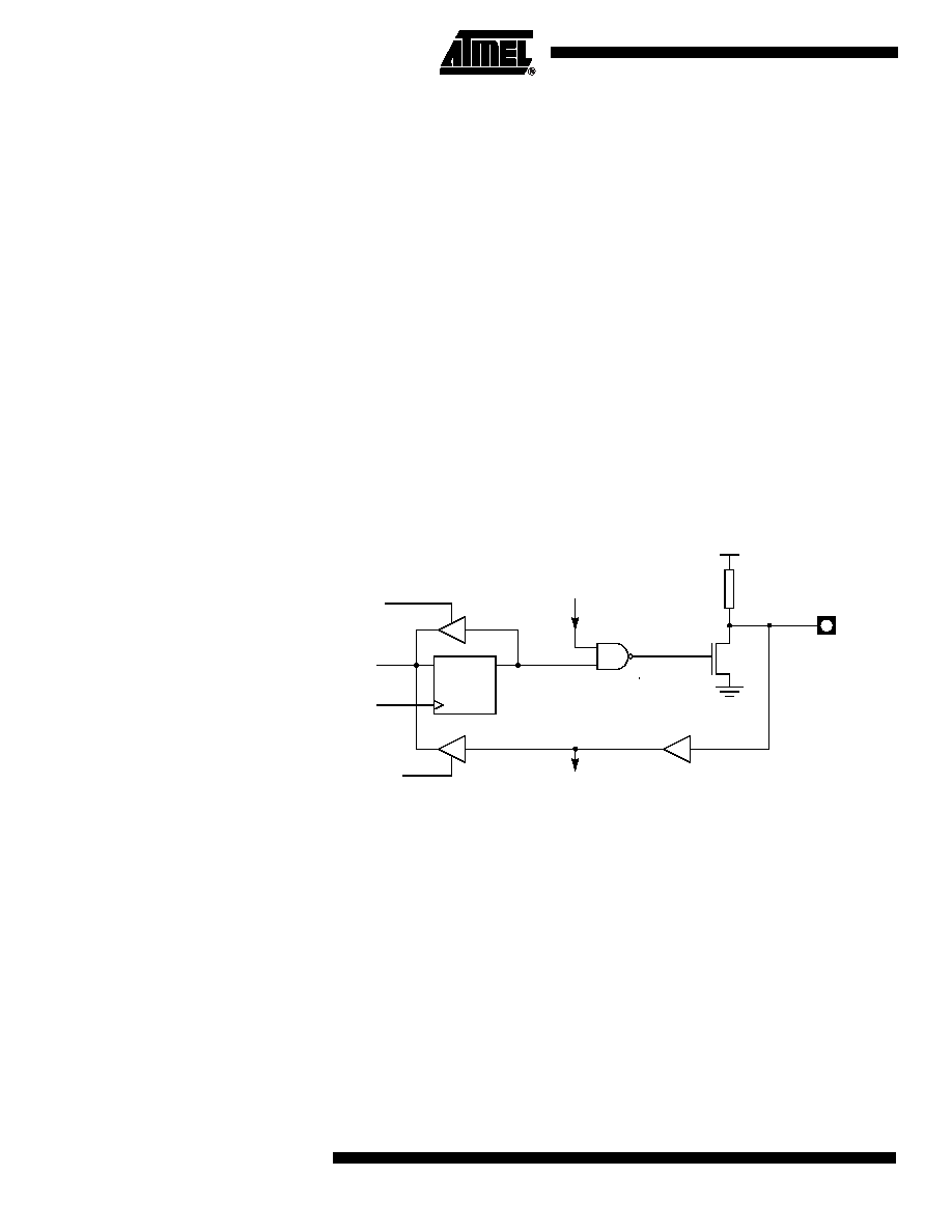
I/O Configurations
Each Port SFR operates via type-D latches, as illustrated in Figure 1 for Ports 3 and 4. A
CPU "write to latch" signal initiates transfer of internal bus data into the type-D latch. A
CPU "read latch" signal transfers the latched Q output onto the internal bus. Similarly, a
"read pin" signal transfers the logical level of the Port pin. Some Port data instructions
activate the "read latch" signal while others activate the "read pin" signal. Latch instruc-
tions are referred to as Read-Modify-Write instructions. Each I/O line may be
independently programmed as input or output.
Port 1, Port 3 and Port 4
Figure 1 shows the structure of Ports 1 and 3, which have internal pull-ups. An external
source can pull the pin low. Each Port pin can be configured either for general-purpose
I/O or for its alternate input output function.
To use a pin for general-purpose output, set or clear the corresponding bit in the Px reg-
ister (x = 1,3 or 4). To use a pin for general-purpose input, set the bit in the Px register.
This turns off the output FET drive.
To configure a pin for its alternate function, set the bit in the Px register. When the latch
is set, the "alternate output function" signal controls the output level (see Figure 1). The
operation of Ports 1, 3 and 4 is discussed further in the "quasi-Bidirectional Port Opera-
tion" section.
Figure 1. Port 1, Port 3 and Port 4 Structure
Note:
The internal pull-up can be disabled on P1 when analog function is selected.
Port 0 and Port 2
Ports 0 and 2 are used for general-purpose I/O or as the external address/data bus. Port
shows the structure of Port 2. An external source can pull a Port 2 pin low.
To use a pin for general-purpose output, set or clear the corresponding bit in the Px reg-
ister (x = 0 or 2). To use a pin for general-purpose input, set the bit in the Px register to
turn off the output driver FET.
D
CL
Q
P1.X
LATCH
INTERNAL
WRITE
TO
LATCH
READ
PIN
READ
LATCH
P1.x
P3.X
P4.X
ALTERNATE
OUTPUT
FUNCTION
VCC
INTERNAL
PULL-UP (1)
ALTERNATE
INPUT
FUNCTION
P3.x
P4.x
BUS
相关PDF资料 |
PDF描述 |
|---|---|
| T89C51CC01UA-RLTIM | IC 8051 MCU FLASH 32K 44VQFP |
| T89C51CC01CA-SLSIM | IC 8051 MCU FLASH 32K 44PLCC |
| T89C51CC01CA-RLTIM | IC 8051 MCU FLASH 32K 44VQFP |
| AT91M55800A-33CI | IC ARM MCU 33MHZ 176-BGA |
| 10FMN-BMTR-A-TB | CONN FMN HSNG 10POS SGL REV SMD |
相关代理商/技术参数 |
参数描述 |
|---|---|
| T89C51CC02 | 制造商:ATMEL 制造商全称:ATMEL Corporation 功能描述:Enhanced 8-bit Microcontroller with CAN Controller and Flash |
| T89C51CC02_03 | 制造商:ATMEL 制造商全称:ATMEL Corporation 功能描述:CAN Microcontrollers |
| T89C51CC02_0305 | 制造商:ATMEL 制造商全称:ATMEL Corporation 功能描述:Enhanced 8-bit Microcontroller with CAN Controller and Flash Memory |
| T89C51CC02_0312 | 制造商:ATMEL 制造商全称:ATMEL Corporation 功能描述:CAN Microcontrollers |
| T89C51CC02_06 | 制造商:ATMEL 制造商全称:ATMEL Corporation 功能描述:Enhanced 8-bit Microcontroller with CAN Controller and Flash |
发布紧急采购,3分钟左右您将得到回复。