- 您现在的位置:买卖IC网 > PDF目录98152 > TA1310ANG SPECIALTY CONSUMER CIRCUIT, PDIP56 PDF资料下载
参数资料
| 型号: | TA1310ANG |
| 元件分类: | 消费家电 |
| 英文描述: | SPECIALTY CONSUMER CIRCUIT, PDIP56 |
| 封装: | 0.600 INCH, 1.78 MM PITCH, PLASTIC, SDIP-56 |
| 文件页数: | 51/106页 |
| 文件大小: | 2686K |
| 代理商: | TA1310ANG |
第1页第2页第3页第4页第5页第6页第7页第8页第9页第10页第11页第12页第13页第14页第15页第16页第17页第18页第19页第20页第21页第22页第23页第24页第25页第26页第27页第28页第29页第30页第31页第32页第33页第34页第35页第36页第37页第38页第39页第40页第41页第42页第43页第44页第45页第46页第47页第48页第49页第50页当前第51页第52页第53页第54页第55页第56页第57页第58页第59页第60页第61页第62页第63页第64页第65页第66页第67页第68页第69页第70页第71页第72页第73页第74页第75页第76页第77页第78页第79页第80页第81页第82页第83页第84页第85页第86页第87页第88页第89页第90页第91页第92页第93页第94页第95页第96页第97页第98页第99页第100页第101页第102页第103页第104页第105页第106页
TA1310ANG
2005-09-20
49
(#16 VCC = 9 V, #37 VCC = 9 V, #51 VCC = 5 V, Ta = 25 ± 3°C)
SW MODE
NOTE
ITEM
SW45 SW46
MEASUREMENT METHOD
C10
Color Difference Output
Voltage Difference in 1H
Period
B
ON
1)
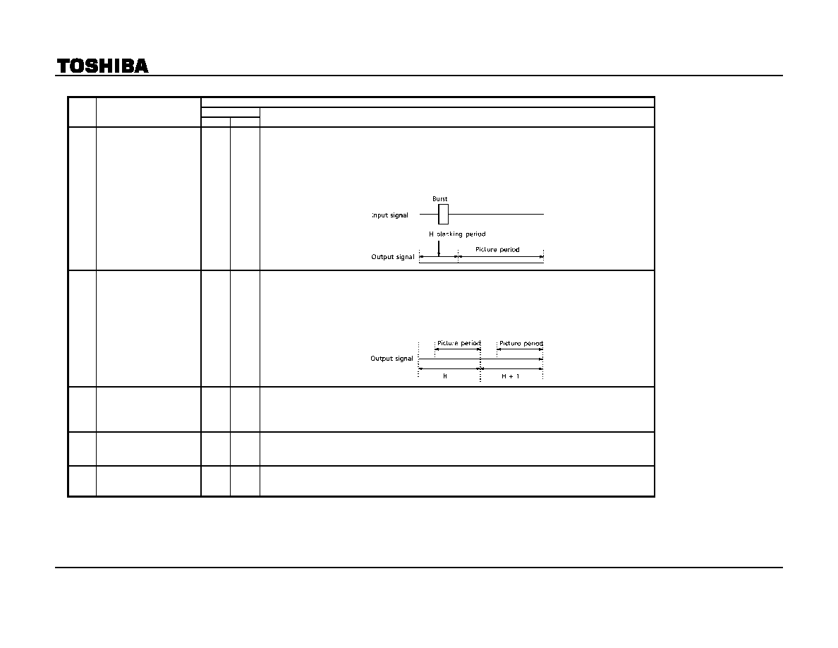
Input no more than 300-mVp-p as a burst signal to chroma input pin (TP45).
2)
Measure the DC voltage difference (vBH) between the H blanking period and picture period of the B-Y
output pin (TP47).
3)
Measure the DC voltage difference (vRH) between the H blanking period and picture period of the R-Y
output pin (TP48).
C11
Color Difference Output
Voltage Difference Every
1H Period
B
ON
1)
Input no more than 300-mVp-p as a burst signal to chroma input pin (TP45).
2)
Measure the DC voltage difference (vBG) between the H picture period and H + 1 picture period of the
B-Y output pin (TP47).
3)
Measure the DC voltage difference (vRG) between the H picture period and H + 1 picture period of the
R-Y output pin (TP48).
C12
Color Difference Output DC
Voltage
B
ON
1)
Input no more than 300-mVp-p as a burst signal to chroma input pin (TP45).
2)
Measure the picture period DC voltage VB of the B-Y output pin (TP47).
3)
Measure the picture period DC voltage VR of the R-Y output pin (TP48).
C13
Difference between DC
Voltage Axes of Color
Difference Output
B
ON
1)
Use the following formula to calculate the difference (VRB) between the voltage axes from the following
formula using the values obtained in C12 above.
VRB = VR VB
C14 X’tal Free-Run Frequency
A
ON
1)
No signal input to the chroma input pin (TP45) (set SW45 to A).
2)
Observe the CW output pin (TP50) and measure the output frequency Xf.
Note 1: Where the bus data are not specified, set the preset values.
Note 2: Ensure the sync signal is always input to TP38 (SYNC IN).
相关PDF资料 |
PDF描述 |
|---|---|
| TA1310AN | SPECIALTY CONSUMER CIRCUIT, PDIP56 |
| TA1310BN | SPECIALTY CONSUMER CIRCUIT, PDIP56 |
| TA1310N | SPECIALTY CONSUMER CIRCUIT, PDIP56 |
| TA1316AN | SPECIALTY CONSUMER CIRCUIT, PDIP56 |
| TA1317AFG | HORIZ/VERT DEFLECTION IC, PDSO30 |
相关代理商/技术参数 |
参数描述 |
|---|---|
| TA1310BM | 制造商:Panasonic Industrial Company 功能描述:SUB ONLY IC |
| TA1310BN | 制造商:Panasonic Industrial Company 功能描述:SUB ONLY IC/P-TA1310DN SUBBING WITH TA1310DN |
| TA1310DN | 制造商:Panasonic Industrial Company 功能描述:IC |
| TA1310N | 制造商:TOSHIBA 制造商全称:Toshiba Semiconductor 功能描述:NTSC VIDEO, CHROMA, DEFRECTION, AND DEC. DISTORTION COMPENSATION IC (FOR YUV INTERFACE AND ACB WITH) |
| TA131308 | 制造商:Fibox 功能描述:Bulk |
发布紧急采购,3分钟左右您将得到回复。