- 您现在的位置:买卖IC网 > PDF目录98161 > TAS5122DFDR (TEXAS INSTRUMENTS INC) 37 W, 2 CHANNEL, AUDIO AMPLIFIER, PDSO56 PDF资料下载
参数资料
| 型号: | TAS5122DFDR |
| 厂商: | TEXAS INSTRUMENTS INC |
| 元件分类: | 音频/视频放大 |
| 英文描述: | 37 W, 2 CHANNEL, AUDIO AMPLIFIER, PDSO56 |
| 封装: | POWERPAD, PLASTIC, TSSOP-56 |
| 文件页数: | 6/22页 |
| 文件大小: | 313K |
| 代理商: | TAS5122DFDR |
TAS5122
SLES088C AUGUST 2003 REVISED NOVEMBER 2003
www.ti.com
14
The AR system is common to both half-bridges.
Timing and Function
Latching Shutdown on All Errors (PMODE1)
In latching shutdown mode all error situations result in a
permanent shutdown (output stage Hi-Z). Re-enabling can
be done by toggling the RESET pin.
All Protection Systems Disabled (PMODE2)
In PMODE2 all protection systems are disabled. This
mode is purely intended for testing and characterization
purposes and thus not recommended for normal device
operation.
MODE Pins Selection
The protection mode is selected by shorting M1/M2 to
DREG or DGND according to Table 2.
Table 2. Protection Mode Selection
M1
M2
PROTECTION MODE
0
Reserved
0
1
Latching shutdown on all errors (PMODE1)
1
0
Reserved
1
Reserved
The output configuration mode is selected by shorting the
M3 pin to DREG or DGND according to Table 3.
Table 3. Output Mode Selection
M3
OUTPUT MODE
0
Bridge-tied load output stage (BTL)
1
Reserved
APPLICATION INFORMATION
DEMODULATION FILTER DESIGN
The TDAA amplifier outputs are driven by heavy-duty
DMOS transistors in an H-bridge configuration. These
transistors are either off or fully on, which reduces the
DMOS transistor on-state resistance, RDSon, and the
power dissipated in the device, thereby increasing
efficiency.
The result is a square-wave output signal with a duty cycle
that is proportional to the amplitude of the audio signal. It
is recommended that a second-order LC filter be used to
recover the audio signal. For this application, EMI is
considered important; therefore, the selected filter is the
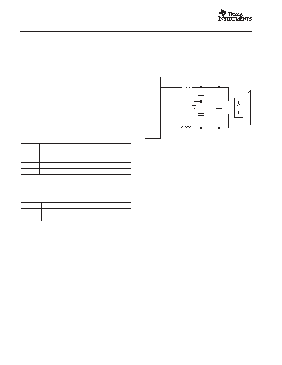
full-output type shown in Figure 10.
Output A
C1A
TAS51xx
L
Output B
L
C1B
C2
R(Load)
Figure 10. Demodulation Filter
The main purpose of the output filter is to attenuate the
high-frequency switching component of the PurePath
Digital amplifier while preserving the signals in the audio
band.
If this rule is observed, the TAS5122 does not have
distortion issues due to the output inductors and
overcurrent conditions do not occur due to inductor
saturation in the output filter.
Another parameter to be considered is the idle current loss
in the inductor. This can be measured or specified as
inductor dissipation (D). The target specification for
dissipation is less than 0.05.
In general, 10-
H inductors suffice for most applications.
The frequency response of the amplifier is slightly altered
by the change in output load resistance; however, unless
very tight control of frequency response is necessary
(better than 0.5 dB), it is not necessary to deviate from
10
H.
The graphs in Figure 11 display the inductance vs current
characteristics of two inductors that are recommended for
use with the TAS5122.
相关PDF资料 |
PDF描述 |
|---|---|
| TAS5132DDVG4 | 50 W, 2 CHANNEL, AUDIO AMPLIFIER, PDSO44 |
| TAS5132DDVRG4 | 50 W, 2 CHANNEL, AUDIO AMPLIFIER, PDSO44 |
| TAS5132DDVR | 50 W, 2 CHANNEL, AUDIO AMPLIFIER, PDSO44 |
| TAS5132DDV | 50 W, 2 CHANNEL, AUDIO AMPLIFIER, PDSO44 |
| TAS5142DKDRG4 | 200 W, 2 CHANNEL, AUDIO AMPLIFIER, PDSO36 |
相关代理商/技术参数 |
参数描述 |
|---|---|
| TAS5122DFDRG4 | 功能描述:音频放大器 Digital Amplifier Power Stage RoHS:否 制造商:STMicroelectronics 产品:General Purpose Audio Amplifiers 输出类型:Digital 输出功率: THD + 噪声: 工作电源电压:3.3 V 电源电流: 最大功率耗散: 最大工作温度: 安装风格:SMD/SMT 封装 / 箱体:TQFP-64 封装:Reel |
| TAS5132 | 制造商:TI 制造商全称:Texas Instruments 功能描述:STEREO DIGITAL AMPLIFIER POWER STAGE |
| TAS5132_07 | 制造商:TI 制造商全称:Texas Instruments 功能描述:STEREO DIGITAL AMPLIFIER POWER STAGE |
| TAS5132_0702 | 制造商:TI 制造商全称:Texas Instruments 功能描述:STEREO DIGITAL AMPLIFIER POWER STAGE |
| TAS5132DDV | 功能描述:音频放大器 Stereo 20W Pwrstage RoHS:否 制造商:STMicroelectronics 产品:General Purpose Audio Amplifiers 输出类型:Digital 输出功率: THD + 噪声: 工作电源电压:3.3 V 电源电流: 最大功率耗散: 最大工作温度: 安装风格:SMD/SMT 封装 / 箱体:TQFP-64 封装:Reel |
发布紧急采购,3分钟左右您将得到回复。