- 您现在的位置:买卖IC网 > PDF目录98182 > TC835C/PI 1-CH 4-BIT DUAL-SLOPE ADC, PARALLEL ACCESS, PDIP28 PDF资料下载
参数资料
| 型号: | TC835C/PI |
| 元件分类: | ADC |
| 英文描述: | 1-CH 4-BIT DUAL-SLOPE ADC, PARALLEL ACCESS, PDIP28 |
| 封装: | 0.600 INCH, PLASTIC, DIP-28 |
| 文件页数: | 2/26页 |
| 文件大小: | 420K |
| 代理商: | TC835C/PI |
TC835
DS21478C-page 10
2007 Microchip Technology Inc.
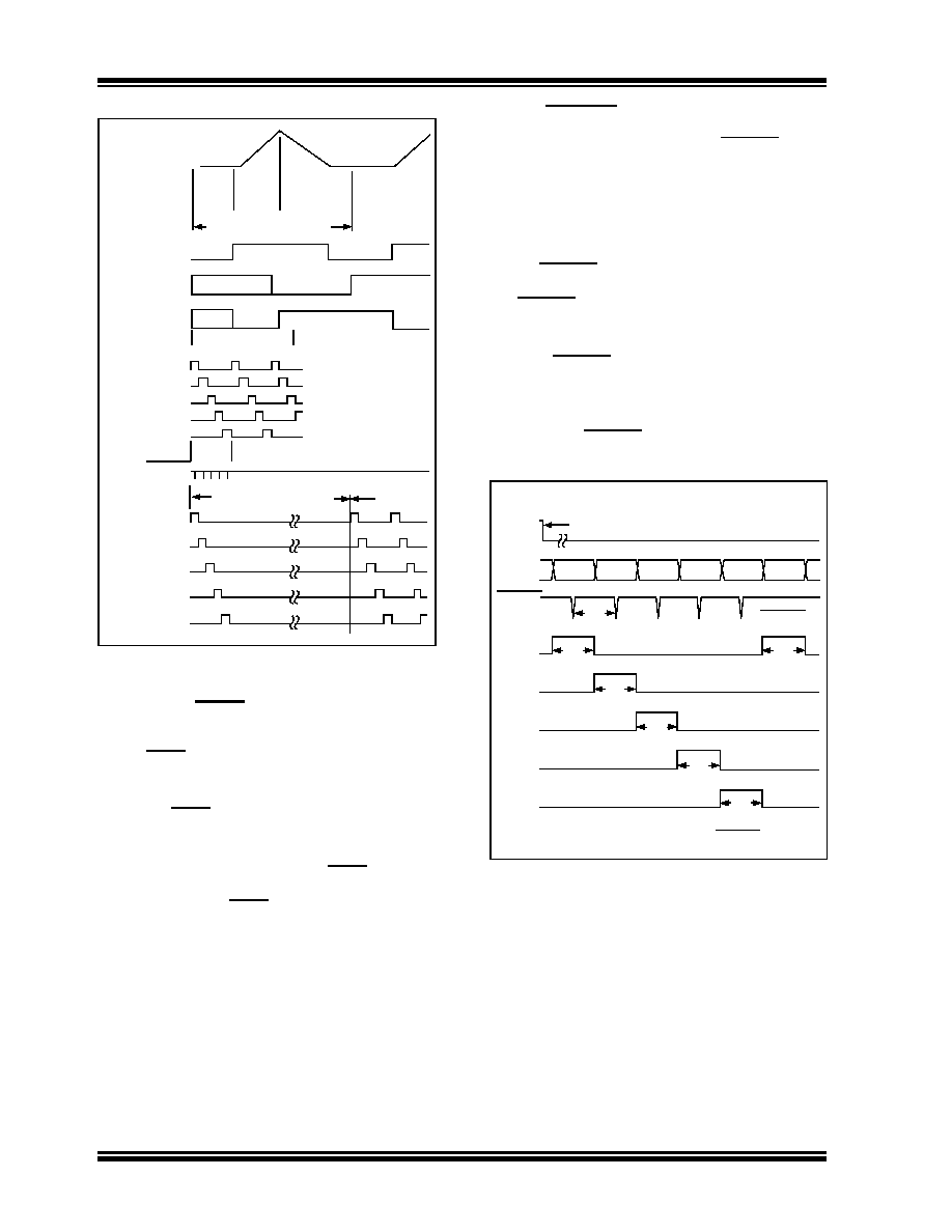
FIGURE 5-2:
Timing Diagrams for
Outputs.
5.1
RUN/HOLD Input
When left open, this pin assumes a logic "1" level. With
a RUN/HOLD = 1, the TC835 performs conversions
continuously, with a new measurement cycle beginning
every 40,002 clock pulses.
When RUN/HOLD changes to a logic "0," the measure-
ment cycle in progress will be completed, and data held
and displayed as long as the logic "0" condition exists.
A positive pulse (> 300 ns) at RUN/HOLD initiates a
new measurement cycle. The measurement cycle in
progress when RUN/HOLD initially assumed the logic
"0" state must be completed before the positive pulse
can be recognized as a single conversion run
command.
The
new
measurement
cycle
begins
with
a
10,001-count auto zero phase. At the end of this phase,
the busy signal goes high.
5.2
STROBE Output
During the measurement cycle, the STROBE control
line is pulsed low five times. The five low pulses occur
in the center of the digit drive signals (D1, D2, D3, D5)
(see Figure 5-3).
D
5 (MSD) goes high for 201 counts when the measure-
ment cycles end. In the center of the D5 pulse, 101
clock pulses after the end of the measurement cycle,
the first STROBE occurs for one-half clock pulse. After
the D5 digit strobe, D4 goes high for 200 clock pulses.
The STROBE goes low 100 clock pulses after D4 goes
high. This continues through the D1 digit drive pulse.
The digit drive signals will continue to permit display
scanning. STROBE pulses are not repeated until a new
measurement is completed. The digit drive signals will
not continue if the previous signal resulted in an
overrange condition.
The active low STROBE pulses aid BCD data transfer
to UARTs, processors and external latches.
FIGURE 5-3:
Strobe Signal Low Five
Times Per Conversion.
5.3
BUSY Output
At the beginning of the signal integration phase, BUSY
goes high and remains high until the first clock pulse
after the integrator zero crossing. BUSY returns to the
logic "0" state after the measurement cycle ends in an
overrange condition. The internal display latches are
loaded during the first clock pulse after BUSY and are
latched at the clock pulse end. The BUSY signal does
not go high at the beginning of the measurement cycle,
which starts with the auto zero cycle.
Integrator
Output
Overrange when
Applicable
Underrange when
Applicable
System
Zero
10,001
Counts
Signal
Integrate
10,000
Counts
(Fixed)
Reference
Integrate
20,001
Counts (Max)
Full Measurement Cycle
40,002 Counts
Busy
Expanded Scale Below
D5
D4
D3
D2
D1
100
Counts
Digit Scan
STROBE
Auto-Zero
Signal
Integrate
Reference
Integrate
D5
D4
D3
D2
D1
Digit Scan
for Overrange
* First D5 of System Zero and
Reference Integrate One Count
Longer
*
End of Conversion
(MSD)
Data
Busy
B1 B8
STROBE
D5
D4
D3
D2
D1
D4
Data
D3
Data
D2
Data
(LSD)
Data
D5
Data
Note Absence
of STROBE
201
Counts
200
Counts
200
Counts
200
Counts
200
Counts
200
Counts
200
Counts
*
*Delay between Busy going Low and First STROBE pulse is
dependent on Analog Input.
TC835
Outputs
D5
D1
相关PDF资料 |
PDF描述 |
|---|---|
| TC835CBUTR | 1-CH DUAL-SLOPE ADC, PQFP64 |
| TC835CBU | 1-CH DUAL-SLOPE ADC, PQFP64 |
| TC835CKWTR | 1-CH DUAL-SLOPE ADC, PQFP44 |
| TC835CKW | 1-CH DUAL-SLOPE ADC, PQFP44 |
| TC835CPIG | 1-CH DUAL-SLOPE ADC, PDIP28 |
相关代理商/技术参数 |
参数描述 |
|---|---|
| TC8395-90 | 制造商:未知厂家 制造商全称:未知厂家 功能描述:16-Bit Microcontroller |
| TC8395BH | 制造商:未知厂家 制造商全称:未知厂家 功能描述:16-Bit Microcontroller |
| TC83C251SA16 | 制造商:INTEL 制造商全称:Intel Corporation 功能描述:HIGH-PERFORMANCE CHMOS MICROCONTROLLER |
| TC83C251SB16 | 制造商:INTEL 制造商全称:Intel Corporation 功能描述:HIGH-PERFORMANCE CHMOS MICROCONTROLLER |
| TC83C251SP16 | 制造商:INTEL 制造商全称:Intel Corporation 功能描述:HIGH-PERFORMANCE CHMOS MICROCONTROLLER |
发布紧急采购,3分钟左右您将得到回复。