- 您现在的位置:买卖IC网 > PDF目录98182 > TC835C/PI 1-CH 4-BIT DUAL-SLOPE ADC, PARALLEL ACCESS, PDIP28 PDF资料下载
参数资料
| 型号: | TC835C/PI |
| 元件分类: | ADC |
| 英文描述: | 1-CH 4-BIT DUAL-SLOPE ADC, PARALLEL ACCESS, PDIP28 |
| 封装: | 0.600 INCH, PLASTIC, DIP-28 |
| 文件页数: | 4/26页 |
| 文件大小: | 420K |
| 代理商: | TC835C/PI |
TC835
DS21478C-page 12
2007 Microchip Technology Inc.
6.0
TYPICAL APPLICATIONS
6.1
Component Value Selection
The integrating resistor is determined by the full-scale
input voltage and the output current of the buffer used
to charge the integrator capacitor. Both the buffer
amplifier and the integrator have a class A output
stage, with 100 A of quiescent current. A 20 A drive
current gives negligible linearity errors. Values of 5 A
to 40 A give good results. The exact value of an
integrating resistor for a 20 A current is easily
calculated.
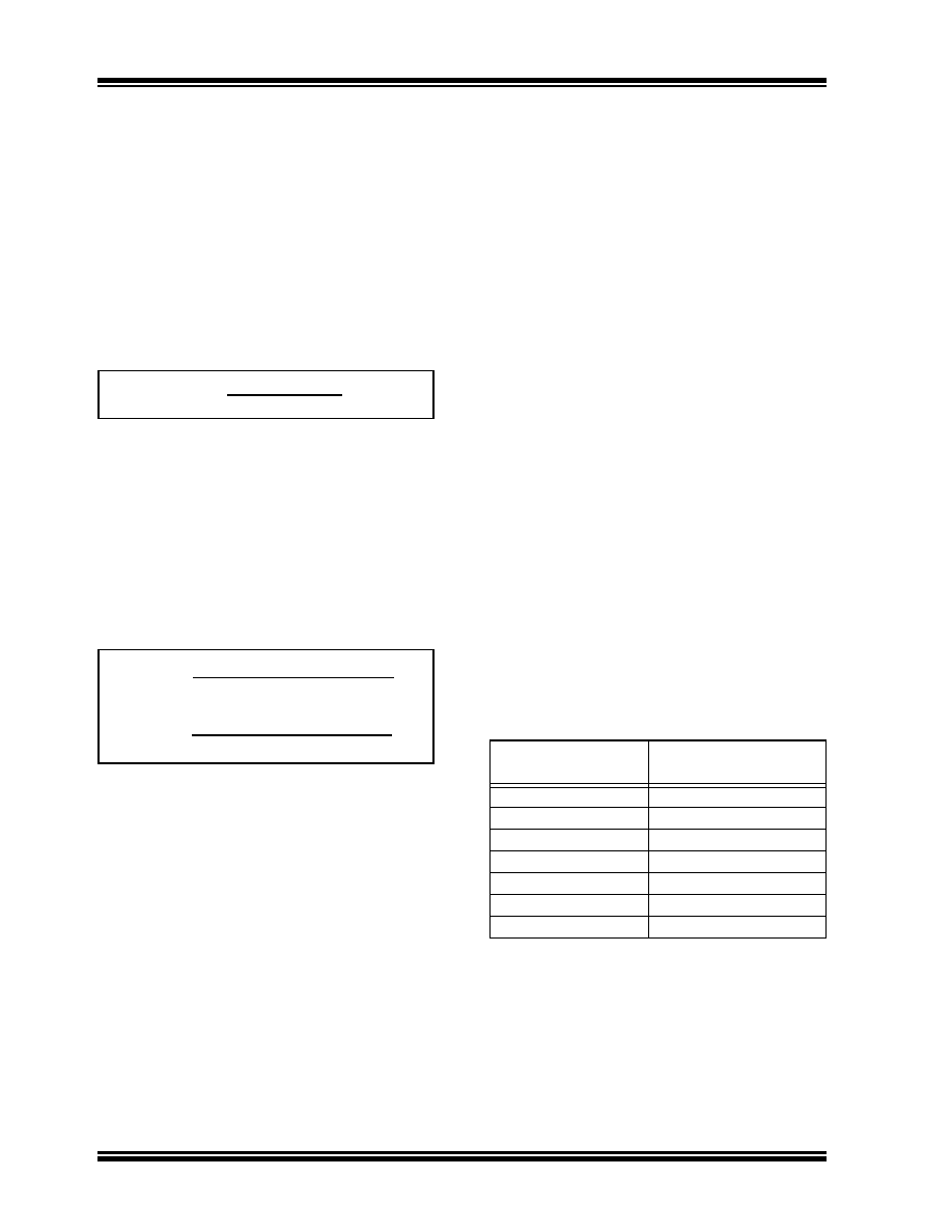
EQUATION 6-1:
6.1.1
INTEGRATING CAPACITOR
The product of integrating resistor and capacitor should
be selected to give the maximum voltage swing that
ensures the tolerance buildup will not saturate the
integrator swing (approximately 0.3V from either
supply). For ±5V supplies and ANALOG COMMON tied
to supply ground, a ±3.5V to ±4V full-scale integrator
swing
is
adequate.
A
0.10 F
to
0.47 F
is
recommended. In general, the value of CINT is given
by:
EQUATION 6-2:
A very important characteristic of the integrating
capacitor is that it has low dielectric absorption to
prevent rollover or ratiometric errors. A good test for
dielectric absorption would be to use the capacitor with
the input tied to the reference. This ratiometric
condition should read half scale 0.9999, with any
deviation
probably
due
to
dielectric
absorption.
Polypropylene capacitors give undetectable errors at
reasonable
cost.
Polystyrene
and
polycarbonate
capacitors
may
also
be
used
in
less
critical
applications.
6.1.2
AUTO ZERO AND REFERENCE
CAPACITORS
The size of the auto zero capacitor has some influence
on the noise of the system. A large capacitor reduces
the noise. The reference capacitor should be large
enough such that stray capacitance to ground from its
nodes is negligible.
The dielectric absorption of the reference capacitor and
auto zero capacitor are only important at power-on or
when the circuit is recovering from an overload.
Smaller or cheaper capacitors can be used if accurate
readings are not required for the first few seconds of
recovery.
6.1.3
REFERENCE VOLTAGE
The analog input required to generate a full scale
output is VIN = 2VREF.
The stability of the reference voltage is a major factor in
the overall absolute accuracy of the converter. For this
reason, it is recommended that a high-quality reference
be used where high-accuracy absolute measurements
are being made.
6.2
Conversion Timing
6.2.1
LINE FREQUENCY REJECTION
A signal integration period at a multiple of the 60Hz line
frequency will maximize 60Hz "line noise" rejection. A
200 kHz clock frequency will reject 60Hz and 400Hz
noise. This corresponds to five readings per second
TABLE 6-1:
CONVERSION RATE VS.
CLOCK FREQUENCY
RINT =
Full scale voltage
20A
CINT =
[10,000 x clock period] x IINT
Integrator output voltage swing
=
(10,000) (clock period) (20
μA)
Integrator output voltage swing
Oscillator Frequency
(kHz)
Conversion Rate
(Conv./Sec.)
100
2.5
120
3
200
5
300
7.5
400
10
800
20
1200
30
相关PDF资料 |
PDF描述 |
|---|---|
| TC835CBUTR | 1-CH DUAL-SLOPE ADC, PQFP64 |
| TC835CBU | 1-CH DUAL-SLOPE ADC, PQFP64 |
| TC835CKWTR | 1-CH DUAL-SLOPE ADC, PQFP44 |
| TC835CKW | 1-CH DUAL-SLOPE ADC, PQFP44 |
| TC835CPIG | 1-CH DUAL-SLOPE ADC, PDIP28 |
相关代理商/技术参数 |
参数描述 |
|---|---|
| TC8395-90 | 制造商:未知厂家 制造商全称:未知厂家 功能描述:16-Bit Microcontroller |
| TC8395BH | 制造商:未知厂家 制造商全称:未知厂家 功能描述:16-Bit Microcontroller |
| TC83C251SA16 | 制造商:INTEL 制造商全称:Intel Corporation 功能描述:HIGH-PERFORMANCE CHMOS MICROCONTROLLER |
| TC83C251SB16 | 制造商:INTEL 制造商全称:Intel Corporation 功能描述:HIGH-PERFORMANCE CHMOS MICROCONTROLLER |
| TC83C251SP16 | 制造商:INTEL 制造商全称:Intel Corporation 功能描述:HIGH-PERFORMANCE CHMOS MICROCONTROLLER |
发布紧急采购,3分钟左右您将得到回复。