- 您现在的位置:买卖IC网 > PDF目录98183 > TC90A80N Y/C SEPARATOR IC, PDIP28 PDF资料下载
参数资料
| 型号: | TC90A80N |
| 元件分类: | 信号分离 |
| 英文描述: | Y/C SEPARATOR IC, PDIP28 |
| 封装: | 0.400 INCH, 1.78 MM PITCH, PLASTIC, SDIP-28 |
| 文件页数: | 7/23页 |
| 文件大小: | 378K |
| 代理商: | TC90A80N |
TC90A80N/F
2002-12-04
15
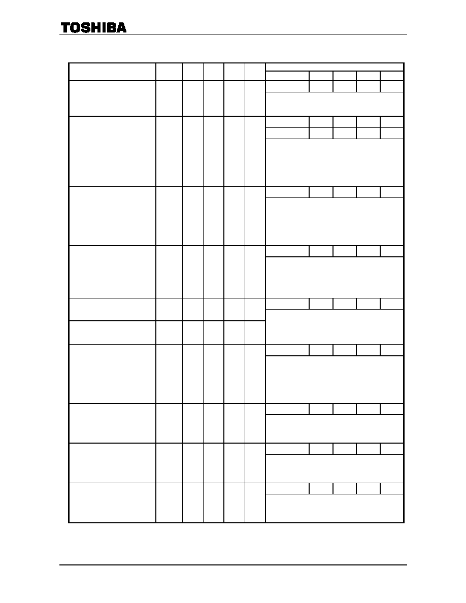
Chrominance signal input/output characteristics
(Ta = 25°C, VDD = 5.00 V, clock input: 3.579545 MHz, 0.5 Vp-p, I
2C bus: according to test conditions)
Test Conditions (Remarks)
Characteristics
Symbol
Min
Typ.
Max
Unit
I2C bus setup
DATA1 DATA2 DATA3 DATA4
I
2C bus setup
8 0
0 0
Recommended input level
VCIN
―
1.0
1.3
V
Input signal : Apply chroma 100% signal to pin 4.
(To pin 4, chrominance signal only;
to pin 9, composite video signal)
I2C bus setup
0 0
I2C bus setup
8 0
0 0
Chrominance signal gain
GC
4.5
5.2
5.8
dB
Input signal : Apply chroma 100%, 0.714-Vp-p
signal to pins 4 and 9. (To pin 4,
chrominance signal only; to pin 9,
composite video signal)
Test content : Compare pin 27 output level with
input level.
I
2C bus setup
0 0
Comb characteristic
Ccom
35
40
―
dB
Input signal : Apply 0.714-Vp-p, 2.5-V DC offset
sine wave to pin 9.
Test content : Monitor pin 27. Change input
frequency. Measure gain difference
between 3.57168 MHz and
3.579545 MHz.
I
2C bus setup
8 0
0 0
BPF frequency characteristic
BWC
0.5
0.2
0
dB
Input signal : Apply 0.714-Vp-p sine wave to pin 4.
Test content : Monitor pin 27. Change input
frequency. Measure gain difference
between 3.579545 MHz and
3.079545 MHz.
I
2C bus setup
0 0
Differential gain
DG
0
2
5
%
Differential phase
DP
0
2
5
°
Input signal : Apply 1-Vp-p, 5-step staircase (0 =
40 IRE) to pin 9.
Test content : Monitor pin 27 using vector scope
(p-p value).
I
2C bus setup
8 0
0 0
Output impedance
Zc
250
400
700
Input signal : Apply 1-Vp-p chroma 100% signal to
pin 4.
Test content : Calculate output impedance, AC
applied with/without 300- resistor
connected between pin 27 and
GND.
I2C bus setup
0 0
Fundamental wave clock
leakage
L1fc
―
0.3
1.0
mVrms Input signal : No input to pin 9.
Test content : Measure fsc (3.579545 MHz)
component of pin 27.
I
2C bus setup
0 0
Clock leakage 1
L4fc
―
4
―
mVrms Input signal : No input to pin 9.
Test content : Measure 4fsc (14.31818 MHz)
component of pin 27.
I
2C bus setup
0 0
Clock leakage 2
L8fc
―
20
―
mVrms Input signal : No input to pin 9.
Test content : Measure 8fsc (28.63636 MHz)
component of pin 27.
相关PDF资料 |
PDF描述 |
|---|---|
| TC90A92AFG | SPECIALTY CONSUMER CIRCUIT, PQFP100 |
| TC9163AN | SPECIALTY ANALOG CIRCUIT, PDIP28 |
| TC9164AF | SPECIALTY ANALOG CIRCUIT, PDSO28 |
| TC9162AF | SPECIALTY ANALOG CIRCUIT, PDSO28 |
| TC9181P | PLL FREQUENCY SYNTHESIZER, 10 MHz, PDIP18 |
相关代理商/技术参数 |
参数描述 |
|---|---|
| TC90A92AFG | 制造商:TOSHIBA 制造商全称:Toshiba Semiconductor 功能描述:3D comb & Video Decoder |
| TC90L01NG | 制造商:TOSHIBA 制造商全称:Toshiba Semiconductor 功能描述:Audio/Video Switching IC for TVs |
| TC9106BP | 制造商:TOSHIBA 制造商全称:Toshiba Semiconductor 功能描述:TC9106BP CB TRANSCEIVER PLL FREQUENCY SYNTHESIZER |
| TC9109BP | 制造商:TOSHIBA 制造商全称:Toshiba Semiconductor 功能描述:TC9109BP CB TRANSCEIVER PLL FREQUENCY SYNTHESIZER |
| TC911 | 制造商:TELCOM 制造商全称:TelCom Semiconductor, Inc 功能描述:AUTO-ZEROED OPERATIONAL AMPLIFIERS |
发布紧急采购,3分钟左右您将得到回复。