- 您现在的位置:买卖IC网 > PDF目录98217 > THS10082IDAG4 (TEXAS INSTRUMENTS INC) 2-CH 10-BIT PROPRIETARY METHOD ADC, PARALLEL ACCESS, PDSO32 PDF资料下载
参数资料
| 型号: | THS10082IDAG4 |
| 厂商: | TEXAS INSTRUMENTS INC |
| 元件分类: | ADC |
| 英文描述: | 2-CH 10-BIT PROPRIETARY METHOD ADC, PARALLEL ACCESS, PDSO32 |
| 封装: | GREEN, PLASTIC, TSSOP-32 |
| 文件页数: | 32/37页 |
| 文件大小: | 350K |
| 代理商: | THS10082IDAG4 |
第1页第2页第3页第4页第5页第6页第7页第8页第9页第10页第11页第12页第13页第14页第15页第16页第17页第18页第19页第20页第21页第22页第23页第24页第25页第26页第27页第28页第29页第30页第31页当前第32页第33页第34页第35页第36页第37页
THS10082
SLAS254B MAY 2002 REVISED NOVEMBER 2002
www.ti.com
4
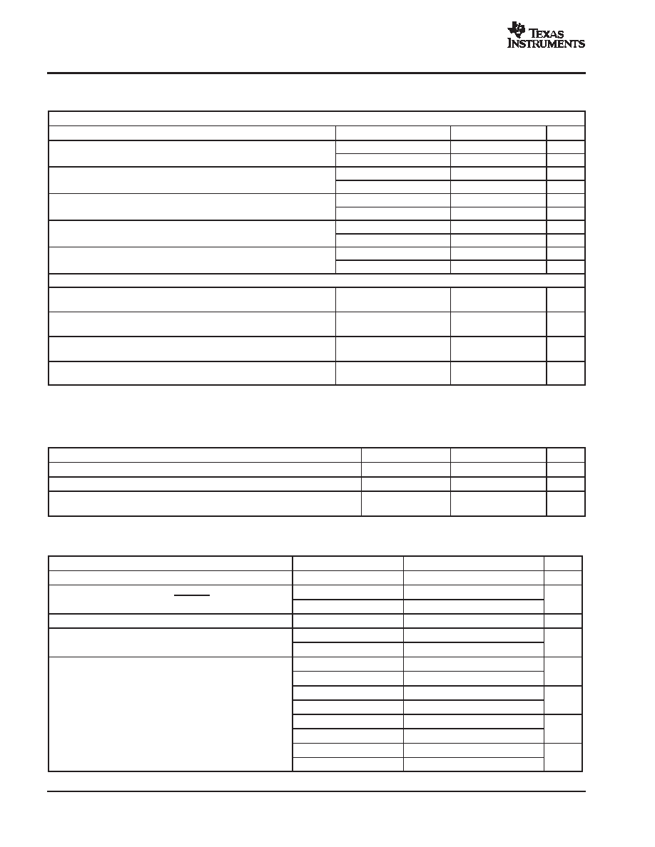
ELECTRICAL CHARACTERISTICS
over recommended operating conditions, VREF = internal, fs = 8 MHz, fI = 2 MHz at 1 dB (unless otherwise noted)
AC SPECIFICATIONS, AVDD = 5 V, BVDD = DVDD = 3.3 V, CL < 30 pF
PARAMETER
TEST CONDITIONS
MIN
TYP
MAX
UNIT
SINAD
Signal-to-noise ratio + distortion
Differential mode
56
59
dB
SINAD
Signal-to-noise ratio + distortion
Single-ended mode(1)
55
58
dB
SNR
Signal-to-noise ratio
Differential mode
59
61
dB
SNR
Signal-to-noise ratio
Single-ended mode(1)
60
dB
THD
Total harmonic distortion
Differential mode
67
61
dB
THD
Total harmonic distortion
Single-ended mode
63
dB
ENOB
Effective number of bits
Differential mode
9
9.5
Bits
ENOB
Effective number of bits
Single-ended mode(1)
9.35
Bits
SFDR
Spurious free dynamic range
Differential mode
61
65
dB
SFDR
Spurious free dynamic range
Single-ended mode
64
dB
Analog Input
Full-power bandwidth with a source impedance of 150
in
differential configuration.
Full-scale sinewave, 3 dB
96
MHz
Full-power bandwidth with a source impedance of 150
in
single-ended configuration.
Full-scale sinewave, 3 dB
54
MHz
Small-signal bandwidth with a source impedance of 150
in
differential configuration.
100-mVpp sinewave, 3 dB
96
MHz
Small-signal bandwidth with a source impedance of 150
in
single-ended configuration.
100-mVpp sinewave, 3 dB
54
MHz
(1) The SNR (ENOB) and SINAD is degraded typically by 2 dB in single-ended mode when the reading of data is asynchronous to the sampling
clock.
TIMING REQUIREMENTS(1)
AVDD = DVDD = 5 V, BVDD = 3.3 V, VREF = internal, CL < 30 pF
PARAMETER
TEST CONDITIONS
MIN
TYP
MAX
UNIT
td(DATA_AV)
Delay time
5
ns
td(o)
Delay time
5
ns
tpipe
Latency
5
CONV
CLK
(1) See Figure 27.
TIMING SPECIFICATION OF THE SINGLE CONVERSION MODE(1)
PARAMETER
TEST CONDITIONS
MIN
TYP
MAX
UNIT
tc
Clock cycle of the internal clock oscillator
117
125
133
ns
tw1
Pulse duration, CONVST
One analog input
1.5
×tc
ns
tw1
Pulse duration, CONVST
Two analog inputs
2.5
×tc
ns
td(A)
Aperture time
1
ns
t2
Delay time between consecutive start of
One analog input
2
×tc
ns
t2
Delay time between consecutive start of
single conversion
Two analog inputs
3
×tc
ns
One analog input, TL = 1
6.5
×tc+15
ns
Two analog inputs, TL = 2
7.5
×tc+15
ns
One analog input, TL = 4
3
×t2 +6.5×tc+15
ns
td(DATA_AV)
Delay time, DATA_AV becomes active for the
Two analog inputs, TL = 4
t2 +7.5×tc+15
ns
td(DATA_AV)
Delay time, DATA_AV becomes active for the
trigger level condition: TRIG0 = 1, TRIG1 = 1
One analog input, TL = 8
7
×t2 +6.5×tc+15
ns
trigger level condition: TRIG0 = 1, TRIG1 = 1
Two analog inputs, TL = 8
3
×t2 +7.5×tc+15
ns
One analog input, TL = 14
13
×t2 +6.5×tc+15
ns
Two analog inputs, TL = 12
13
×t2 +6.5×tc+15
ns
(1) See Figure 26.
相关PDF资料 |
PDF描述 |
|---|---|
| THS1009CDAR | 2-CH 10-BIT PROPRIETARY METHOD ADC, PARALLEL ACCESS, PDSO32 |
| THS1009CDA | 2-CH 10-BIT PROPRIETARY METHOD ADC, PARALLEL ACCESS, PDSO32 |
| THS1009IDA | 2-CH 10-BIT PROPRIETARY METHOD ADC, PARALLEL ACCESS, PDSO32 |
| THS1009IDAR | 2-CH 10-BIT PROPRIETARY METHOD ADC, PARALLEL ACCESS, PDSO32 |
| THS1009IDAG4 | 2-CH 10-BIT PROPRIETARY METHOD ADC, PARALLEL ACCESS, PDSO32 |
相关代理商/技术参数 |
参数描述 |
|---|---|
| THS1009 | 制造商:TI 制造商全称:Texas Instruments 功能描述:10-BIT, 2 ANALOG INPUT, 8 MSPS, SIMULTANEOUS SAMPLING ANALOG-TO-DIGITAL CONVERTER |
| THS1009CDA | 制造商:TI 制造商全称:Texas Instruments 功能描述:10-BIT, 2 ANALOG INPUT, 8 MSPS, SIMULTANEOUS SAMPLING ANALOG-TO-DIGITAL CONVERTER |
| THS1009CDAG4 | 制造商:TI 制造商全称:Texas Instruments 功能描述:10-BIT, 2 ANALOG INPUT, 8 MSPS, SIMULTANEOUS SAMPLING ANALOG-TO-DIGITAL CONVERTER |
| THS1009CDAR | 制造商:TI 制造商全称:Texas Instruments 功能描述:10-BIT, 2 ANALOG INPUT, 8 MSPS, SIMULTANEOUS SAMPLING ANALOG-TO-DIGITAL CONVERTER |
| THS1009CDARG4 | 制造商:TI 制造商全称:Texas Instruments 功能描述:10-BIT, 2 ANALOG INPUT, 8 MSPS, SIMULTANEOUS SAMPLING ANALOG-TO-DIGITAL CONVERTER |
发布紧急采购,3分钟左右您将得到回复。