- 您现在的位置:买卖IC网 > PDF目录98218 > THS1041CDWRG4 (TEXAS INSTRUMENTS INC) 1-CH 10-BIT PROPRIETARY METHOD ADC, PARALLEL ACCESS, PDSO28 PDF资料下载
参数资料
| 型号: | THS1041CDWRG4 |
| 厂商: | TEXAS INSTRUMENTS INC |
| 元件分类: | ADC |
| 英文描述: | 1-CH 10-BIT PROPRIETARY METHOD ADC, PARALLEL ACCESS, PDSO28 |
| 封装: | GREEN, PLASTIC, SOIC-28 |
| 文件页数: | 24/41页 |
| 文件大小: | 777K |
| 代理商: | THS1041CDWRG4 |
第1页第2页第3页第4页第5页第6页第7页第8页第9页第10页第11页第12页第13页第14页第15页第16页第17页第18页第19页第20页第21页第22页第23页当前第24页第25页第26页第27页第28页第29页第30页第31页第32页第33页第34页第35页第36页第37页第38页第39页第40页第41页
THS1041
SLAS289C OCTOBER 2001 REVISED OCTOBER 2004
30
www.ti.com
APPLICATION INFORMATION
driving the VREF pin (continued)
Note that the maximum current may be up to 30% higher. The user should ensure that VREF is driven from a
low noise, low drift source, well decoupled to analog ground and capable of driving the maximum IREF.
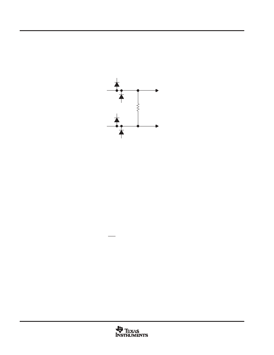
driving REFT and REFB (external ADC references, MODE = AGND)
AVDD
AGND
AVDD
AGND
2 k
REFT
REFB
To ADC Core
Figure 46. Equivalent Circuit of REFT and REFB Inputs
designing the dc clamp
Figure 38 shows the basic operation of the clamp circuit with the analog input AIN+ coupled via an RC circuit.
AIN must be connected to a dc source whose voltage level keeps the THS1041 differential input within the ADC
input range. The clamp voltage output level may be established by an analog voltage on the CLAMPIN pin or
by programming the on-chip clamp DAC.
(Note that it is possible to reverse the AIN+ and AIN connections if signal inversion is also required. The
following section assumes that the signal is coupled to AIN+ and that AIN is connected to a suitable dc bias
level).
initial clamp acquisition time
Acquisition time is the time required to reach the target clamp voltage at AIN+ when the clamp switch SW1 is
closed for the first time. The acquisition time is given by
T
ACQ +
C
IN
R
lN
ln
V
C
V
E
where VC is the difference between the dc level of the input VIN and the target clamp output voltage, VClamp.
VE is the difference between the ideal VC and the actual VC obtained during the acquisition time. The maximum
tolerable error depends on the application requirements.
For example, consider clamping an incoming video signal that has a black level near 0.3 V to a black level of
1.3 V at the THS1041 AIN+ input. The voltage VC required across the input coupling capacitor is thus
1.3 0.3 = 1 V. If a 10 mV or less clamp voltage error VE gives acceptable system operation, the source
resistance RIN is 20 and the coupling capacitor CIN is 1 F, then the total clamp pulse duration required to
reach this error is:
TACQ = 1 F × 20 × ln(1/0.01) = 92 s (approximate)
(16)
相关PDF资料 |
PDF描述 |
|---|---|
| THS1041IDWRG4 | 1-CH 10-BIT PROPRIETARY METHOD ADC, PARALLEL ACCESS, PDSO28 |
| THS1041CDW | 1-CH 10-BIT PROPRIETARY METHOD ADC, PARALLEL ACCESS, PDSO28 |
| THS1041CPW | 1-CH 10-BIT PROPRIETARY METHOD ADC, PARALLEL ACCESS, PDSO28 |
| THS1041IPW | 1-CH 10-BIT PROPRIETARY METHOD ADC, PARALLEL ACCESS, PDSO28 |
| THS1041CDWR | 1-CH 10-BIT PROPRIETARY METHOD ADC, PARALLEL ACCESS, PDSO28 |
相关代理商/技术参数 |
参数描述 |
|---|---|
| THS1041CPW | 功能描述:模数转换器 - ADC 10 Bit 40 MSPS Lo-Pwr RoHS:否 制造商:Texas Instruments 通道数量:2 结构:Sigma-Delta 转换速率:125 SPs to 8 KSPs 分辨率:24 bit 输入类型:Differential 信噪比:107 dB 接口类型:SPI 工作电源电压:1.7 V to 3.6 V, 2.7 V to 5.25 V 最大工作温度:+ 85 C 安装风格:SMD/SMT 封装 / 箱体:VQFN-32 |
| THS1041CPWG4 | 功能描述:模数转换器 - ADC 10 Bit 40 MSPS Lo-Pwr RoHS:否 制造商:Texas Instruments 通道数量:2 结构:Sigma-Delta 转换速率:125 SPs to 8 KSPs 分辨率:24 bit 输入类型:Differential 信噪比:107 dB 接口类型:SPI 工作电源电压:1.7 V to 3.6 V, 2.7 V to 5.25 V 最大工作温度:+ 85 C 安装风格:SMD/SMT 封装 / 箱体:VQFN-32 |
| THS1041CPWR | 功能描述:模数转换器 - ADC 10 Bit 40 MSPS Lo-Pwr RoHS:否 制造商:Texas Instruments 通道数量:2 结构:Sigma-Delta 转换速率:125 SPs to 8 KSPs 分辨率:24 bit 输入类型:Differential 信噪比:107 dB 接口类型:SPI 工作电源电压:1.7 V to 3.6 V, 2.7 V to 5.25 V 最大工作温度:+ 85 C 安装风格:SMD/SMT 封装 / 箱体:VQFN-32 |
| THS1041CPWRG4 | 功能描述:模数转换器 - ADC 10 Bit 40 MSPS Lo-Pwr RoHS:否 制造商:Texas Instruments 通道数量:2 结构:Sigma-Delta 转换速率:125 SPs to 8 KSPs 分辨率:24 bit 输入类型:Differential 信噪比:107 dB 接口类型:SPI 工作电源电压:1.7 V to 3.6 V, 2.7 V to 5.25 V 最大工作温度:+ 85 C 安装风格:SMD/SMT 封装 / 箱体:VQFN-32 |
| THS1041EVM | 功能描述:数据转换 IC 开发工具 THS1041 Eval Mod RoHS:否 制造商:Texas Instruments 产品:Demonstration Kits 类型:ADC 工具用于评估:ADS130E08 接口类型:SPI 工作电源电压:- 6 V to + 6 V |
发布紧急采购,3分钟左右您将得到回复。