- 您现在的位置:买卖IC网 > PDF目录98218 > THS1041CDWRG4 (TEXAS INSTRUMENTS INC) 1-CH 10-BIT PROPRIETARY METHOD ADC, PARALLEL ACCESS, PDSO28 PDF资料下载
参数资料
| 型号: | THS1041CDWRG4 |
| 厂商: | TEXAS INSTRUMENTS INC |
| 元件分类: | ADC |
| 英文描述: | 1-CH 10-BIT PROPRIETARY METHOD ADC, PARALLEL ACCESS, PDSO28 |
| 封装: | GREEN, PLASTIC, SOIC-28 |
| 文件页数: | 38/41页 |
| 文件大小: | 777K |
| 代理商: | THS1041CDWRG4 |
第1页第2页第3页第4页第5页第6页第7页第8页第9页第10页第11页第12页第13页第14页第15页第16页第17页第18页第19页第20页第21页第22页第23页第24页第25页第26页第27页第28页第29页第30页第31页第32页第33页第34页第35页第36页第37页当前第38页第39页第40页第41页
THS1041
SLAS289C OCTOBER 2001 REVISED OCTOBER 2004
6
www.ti.com
electrical characteristics
over recommended operating conditions, AVDD = 3 V, DVDD = 3 V, fs = 40 MSPS/50% duty cycle, MODE = AVDD (internal reference),
differential input range = 1 Vpp and 2 Vpp, PGA = 1X, TA = Tmin to Tmax (unless otherwise noted) (continued)
dynamic performance (ADC and PGA)
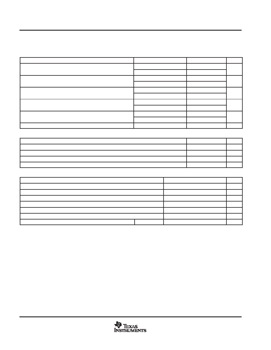
PARAMETER
TEST CONDITIONS
MIN
TYP
MAX
UNIT
ENOB
Effective number of bits
f = 4.8 MHz, 0.5 dBFS
8.8
9.6
Bits
ENOB
Effective number of bits
f = 20 MHz, 0.5 dBFS
9.5
Bits
SFDR
Spurious free dynamic range
f = 4.8 MHz, 0.5 dBFS
60.5
72
dB
SFDR
Spurious free dynamic range
f = 20 MHz, 0.5 dBFS
70
dB
THD
Total harmonic distortion
f = 4.8 MHz, 0.5 dBFS
72.5
61.3
dB
THD
Total harmonic distortion
f = 20 MHz, 0.5 dBFS
71.6
dB
SNR
Signal-to-noise ratio
f = 4.8 MHz, 0.5 dBFS
55.7
60
dB
SNR
Signal-to-noise ratio
f = 20 MHz, 0.5 dBFS
57
dB
SINAD
Signal-to-noise and distortion
f = 4.8 MHz, 0.5 dBFS
55.6
59.7
dB
SINAD
Signal-to-noise and distortion
f = 20 MHz, 0.5 dBFS
59.6
dB
BW
Full power bandwidth (3 dB)
900
MHz
PGA (See Note 7)
PARAMETER
MIN
TYP
MAX
UNIT
Gain range (linear scale)
0.5
4
V/V
Gain step size (linear scale)
0.485
0.5
0.515
V/V
Gain error (deviation from ideal, all gain settings)
3%
Number of control bits
3
Bits
clamp amplifier and clamp DAC (See Note 8)
PARAMETER
MIN
TYP
MAX
UNIT
Resolution
10
Bits
DAC output range
REFB
REFT
V
DAC differential nonlinearity
1
LSB
DAC integral nonlinearity
3
LSB
Clamping analog output voltage range
0.1
AVDD0.1
V
Clamping analog output voltage error
40
mV
Clamping analog output bias voltage
MODE = AVDD AVDD/2 0.1
AVDD/2 + 0.1
mV
NOTES:
7. Gain settings increment by the gain step size for eight binary settings of 000 to 111 to correspond to the ideal gain range.
8. The CLAMPOUT pin must see a load capacitance of at least 10 nF to ensure stability of the on-chip clamp buffer. When using the
clamp for dc restoration, the signal coupling capacitor should be at least 10 nF. When using the clamp buffer as a dc biasing reference,
CLAMPOUT should be decoupled to analog ground through at least a 10-nF capacitor.
相关PDF资料 |
PDF描述 |
|---|---|
| THS1041IDWRG4 | 1-CH 10-BIT PROPRIETARY METHOD ADC, PARALLEL ACCESS, PDSO28 |
| THS1041CDW | 1-CH 10-BIT PROPRIETARY METHOD ADC, PARALLEL ACCESS, PDSO28 |
| THS1041CPW | 1-CH 10-BIT PROPRIETARY METHOD ADC, PARALLEL ACCESS, PDSO28 |
| THS1041IPW | 1-CH 10-BIT PROPRIETARY METHOD ADC, PARALLEL ACCESS, PDSO28 |
| THS1041CDWR | 1-CH 10-BIT PROPRIETARY METHOD ADC, PARALLEL ACCESS, PDSO28 |
相关代理商/技术参数 |
参数描述 |
|---|---|
| THS1041CPW | 功能描述:模数转换器 - ADC 10 Bit 40 MSPS Lo-Pwr RoHS:否 制造商:Texas Instruments 通道数量:2 结构:Sigma-Delta 转换速率:125 SPs to 8 KSPs 分辨率:24 bit 输入类型:Differential 信噪比:107 dB 接口类型:SPI 工作电源电压:1.7 V to 3.6 V, 2.7 V to 5.25 V 最大工作温度:+ 85 C 安装风格:SMD/SMT 封装 / 箱体:VQFN-32 |
| THS1041CPWG4 | 功能描述:模数转换器 - ADC 10 Bit 40 MSPS Lo-Pwr RoHS:否 制造商:Texas Instruments 通道数量:2 结构:Sigma-Delta 转换速率:125 SPs to 8 KSPs 分辨率:24 bit 输入类型:Differential 信噪比:107 dB 接口类型:SPI 工作电源电压:1.7 V to 3.6 V, 2.7 V to 5.25 V 最大工作温度:+ 85 C 安装风格:SMD/SMT 封装 / 箱体:VQFN-32 |
| THS1041CPWR | 功能描述:模数转换器 - ADC 10 Bit 40 MSPS Lo-Pwr RoHS:否 制造商:Texas Instruments 通道数量:2 结构:Sigma-Delta 转换速率:125 SPs to 8 KSPs 分辨率:24 bit 输入类型:Differential 信噪比:107 dB 接口类型:SPI 工作电源电压:1.7 V to 3.6 V, 2.7 V to 5.25 V 最大工作温度:+ 85 C 安装风格:SMD/SMT 封装 / 箱体:VQFN-32 |
| THS1041CPWRG4 | 功能描述:模数转换器 - ADC 10 Bit 40 MSPS Lo-Pwr RoHS:否 制造商:Texas Instruments 通道数量:2 结构:Sigma-Delta 转换速率:125 SPs to 8 KSPs 分辨率:24 bit 输入类型:Differential 信噪比:107 dB 接口类型:SPI 工作电源电压:1.7 V to 3.6 V, 2.7 V to 5.25 V 最大工作温度:+ 85 C 安装风格:SMD/SMT 封装 / 箱体:VQFN-32 |
| THS1041EVM | 功能描述:数据转换 IC 开发工具 THS1041 Eval Mod RoHS:否 制造商:Texas Instruments 产品:Demonstration Kits 类型:ADC 工具用于评估:ADS130E08 接口类型:SPI 工作电源电压:- 6 V to + 6 V |
发布紧急采购,3分钟左右您将得到回复。