- 您现在的位置:买卖IC网 > PDF目录98228 > THS7303PW (TEXAS INSTRUMENTS INC) 3 CHANNEL, VIDEO AMPLIFIER, PDSO20 PDF资料下载
参数资料
| 型号: | THS7303PW |
| 厂商: | TEXAS INSTRUMENTS INC |
| 元件分类: | 音频/视频放大 |
| 英文描述: | 3 CHANNEL, VIDEO AMPLIFIER, PDSO20 |
| 封装: | GREEN, PLASTIC, TSSOP-20 |
| 文件页数: | 15/60页 |
| 文件大小: | 1980K |
| 代理商: | THS7303PW |
第1页第2页第3页第4页第5页第6页第7页第8页第9页第10页第11页第12页第13页第14页当前第15页第16页第17页第18页第19页第20页第21页第22页第23页第24页第25页第26页第27页第28页第29页第30页第31页第32页第33页第34页第35页第36页第37页第38页第39页第40页第41页第42页第43页第44页第45页第46页第47页第48页第49页第50页第51页第52页第53页第54页第55页第56页第57页第58页第59页第60页
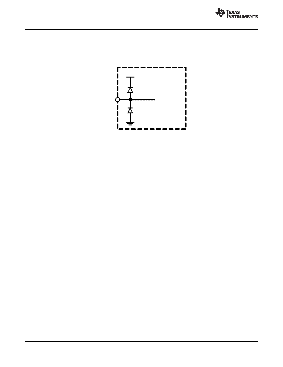
External
Input/
Output
Pin
Internal
Circuitry
VS+
SLOS479B
– OCTOBER 2005 – REVISED MARCH 2011
INPUT OVERVOLTAGE PROTECTION
The THS7303 is built using a high-speed complementary bipolar and CMOS process. The internal junction
breakdown voltages are low for these very small geometry devices. These breakdowns are reflected in the
Absolute Maximum Ratings table. All input and output device pins are protected with internal ESD protection
diodes to the power supplies, as shown in Figure 58.
Figure 58. Internal ESD Protection
These diodes provide moderate protection to input overdrive voltages above and below the supplies. The
protection diodes can typically support 30-mA of continuous current when overdriven.
TYPICAL CONFIGURATION and VIDEO TERMINOLOGY
A typical application circuit using the THS7303 as a video buffer is shown in Figure 59. It shows a DAC (or
encoder such as the THS8200) driving the three input channels of the THS7303. Although the high-definition
video (HD) or enhanced-definition (ED) Y
’P’BP’R (sometimes Y’U’V’ is used or it is incorrectly labeled Y’C’BC’R)
channels are shown, these channels can easily be S-Video Y
’C’ channels and the composite video baseband
signal (CVBS) of a standard definition video (SD) system. These signals can also be G
’B’R’ (R'G'B') signals or
other variations. Note that for computer signals the sync should be embedded within the signal for a system with
only 3-outputs. This is sometimes labeled as R
’G’sB’ (sync on green) or R’sG’sB’s (sync on all signals).
The second set of inputs (B-Channels) shown are being driven from an external input typically used as a
pass-through function. These are either HD, ED, or SD video signals. The flexibility of the THS7303 allows for
almost any input signal to be driven into the THS7303 regardless of the other set of inputs. Control of the I2C
configures each channel of the THS7303 independently of the other channels. For example, the THS7303 can
be configured to have Channel 1 Input connected to input A with 35-MHz LPF while Channels 2 and 3 are
connected to input B with 16-MHz LPF. See the various sections explaining the I2C interface later in this data
sheet for more information.
Note that the Y
’ term is used for the luma channels throughout this document rather than the more common
luminance (Y) term. The reason is to account for the definition of luminance as stipulated by the CIE -
International Commission on Illumination. Video departs from true luminance since a nonlinear term, gamma, is
added to the true RGB signals to form R
’G’B’ signals. These R’G’B’ signals are then used to mathematically
create luma (Y
’). Thus luminance (Y) is not maintained requiring a difference in terminology.
This rationale is also used for the chroma (C
’) term. Chroma is derived from the non-linear R’G’B’ terms and thus
it is nonlinear. Chominance (C) is derived from linear RGB giving the difference between chroma (C
’) and
chrominance (C). The color difference signals (P
’B / P’R / U’ / V’) are also referenced this way to denote the
nonlinear (gamma corrected) signals.
R
’G’B’ (commonly mislabeled RGB) is also called G’B’R’ (again commonly mislabeled as GBR) in professional
video systems. The SMPTE component standard stipulates that the luma information is placed on the first
channel, the blue color difference is placed on the second channel, and the red color difference signal is placed
on the third channel. This is consistent with the Y'P'BP'R nomenclature. Because the luma channel (Y') carries the
sync information and the green channel (G') also carries the sync information, it makes logical sense that G' be
22
Copyright
2005–2011, Texas Instruments Incorporated
Product Folder Link(s): THS7303
相关PDF资料 |
PDF描述 |
|---|---|
| THS7303PWG4 | 3 CHANNEL, VIDEO AMPLIFIER, PDSO20 |
| THS7303PWRG4 | 3 CHANNEL, VIDEO AMPLIFIER, PDSO20 |
| THS7315DR | 3 CHANNEL, VIDEO AMPLIFIER, PDSO8 |
| THS7315D | 3 CHANNEL, VIDEO AMPLIFIER, PDSO8 |
| THS7315DG4 | 3 CHANNEL, VIDEO AMPLIFIER, PDSO8 |
相关代理商/技术参数 |
参数描述 |
|---|---|
| THS7303PWG4 | 功能描述:视频放大器 3-Ch Low Power Video RoHS:否 制造商:ON Semiconductor 通道数量:4 电源类型: 工作电源电压:3.3 V, 5 V 电源电流: 最小工作温度: 最大工作温度: 封装 / 箱体:TSSOP-14 封装:Reel |
| THS7303PWR | 功能描述:视频放大器 3-Ch Low Power Video RoHS:否 制造商:ON Semiconductor 通道数量:4 电源类型: 工作电源电压:3.3 V, 5 V 电源电流: 最小工作温度: 最大工作温度: 封装 / 箱体:TSSOP-14 封装:Reel |
| THS7303PWRG4 | 功能描述:视频放大器 3-Ch Low Power Video RoHS:否 制造商:ON Semiconductor 通道数量:4 电源类型: 工作电源电压:3.3 V, 5 V 电源电流: 最小工作温度: 最大工作温度: 封装 / 箱体:TSSOP-14 封装:Reel |
| THS730A A2 | 制造商:Tektronix Inc 功能描述:OSCILLOSCOPE DSO/DMM 200MHZ |
发布紧急采购,3分钟左右您将得到回复。