- 您现在的位置:买卖IC网 > PDF目录98228 > THS7303PW (TEXAS INSTRUMENTS INC) 3 CHANNEL, VIDEO AMPLIFIER, PDSO20 PDF资料下载
参数资料
| 型号: | THS7303PW |
| 厂商: | TEXAS INSTRUMENTS INC |
| 元件分类: | 音频/视频放大 |
| 英文描述: | 3 CHANNEL, VIDEO AMPLIFIER, PDSO20 |
| 封装: | GREEN, PLASTIC, TSSOP-20 |
| 文件页数: | 26/60页 |
| 文件大小: | 1980K |
| 代理商: | THS7303PW |
第1页第2页第3页第4页第5页第6页第7页第8页第9页第10页第11页第12页第13页第14页第15页第16页第17页第18页第19页第20页第21页第22页第23页第24页第25页当前第26页第27页第28页第29页第30页第31页第32页第33页第34页第35页第36页第37页第38页第39页第40页第41页第42页第43页第44页第45页第46页第47页第48页第49页第50页第51页第52页第53页第54页第55页第56页第57页第58页第59页第60页
17
20
19
18
GND
16
CH.2 IN B
CH.3 IN B
15
I2C-A0
SDA
VS+ 11
14
13
12
SCL
CH. 3 SAG
I2C-A1
CH.1 IN B
CH.2 IN A
CH.3 IN A
CH.1 IN A
NC
CH.3 OUT
CH. 2 SAG
CH.2 OUT
CH. 1 SAG
CH.1 OUT
NC
1
2
3
4
5
6
7
8
9
10
+
DAC /
Encoder
(THS8200)
Y’
P’B
P’R
External
Input
Y’
P’B
P’R
R
HDTV
480i
576i
480p
576p
720p
1080i
1080p
3.3V
75 W
Y’
Out
P’
Out
B
P’
Out
R
75 W
0.1 F
m
0.01 F
m
+Vs
100 F
m
1 F
m
1 F
m
47 F
m
47 F
m
47 F
m
33 F
m
33 F
m
33 F
m
*(SeeNote A)
*
I C
Controller
2
ACSTC
ACBias
DC+135mV
SLOS479B
– OCTOBER 2005 – REVISED MARCH 2011
The internal resistor values were chosen to optimize the system while using the 47-
μF and 33-μF capacitors, and
to approximate the performance of a single 330-
μF capacitor. These capacitors can be a different value if
desired, but the characteristics of the system are altered accordingly. For example, if 22-
μF capacitors are used
for both sections, then there are increases in line tilt and field tilt. For some systems, this may be considered
acceptable (for example, 720p Y' signals with the associated faster line rates). Using larger values, such as 68
μF and 47 μF respectively, decreases field time distortion even further, and approaches the performance of a
single 470-
μF capacitor.
It is important to note that the dc gain is about 2.55 V/V. Thus, if the input has a dc bias, the output dc bias is
2.55 times the input. For example, this results in an output bias point of 355 mV for the dc + 135 mV shift.
Additionally, if the ac bias input mode is selected, the dc operating point is VS+/4 × 2.55, or 2.1 V with 3.3-V
supply and 3.2 V with 5-V supply. This additional offset should not hinder the performance of the THS7303
because there is still plenty of voltage headroom between the dc operating point and the rail-to-rail output
capability.
One possible concern about this configuration is that the low-frequency gain enhancement may cause saturation
of the signal when low power-supply voltages (such as 3 V) are used. The internal resistors were chosen to
minimize the low-frequency gain so that saturation is minimized. Other SAG correction devices have much higher
low-frequency gain (10 dB or higher), which when coupled with low power-supply voltages, can easily create
clipping on the output of the amplifier, both dynamically and at dc. Other SAG correction devices do not use a
resistor in series with the SAG pin. Neglecting this resistor can result in a large Q enhancement causing possible
saturation issues. These systems typically require much larger capacitor values to minimize this problem, which
ultimately minimizes the benefits of SAG correction.
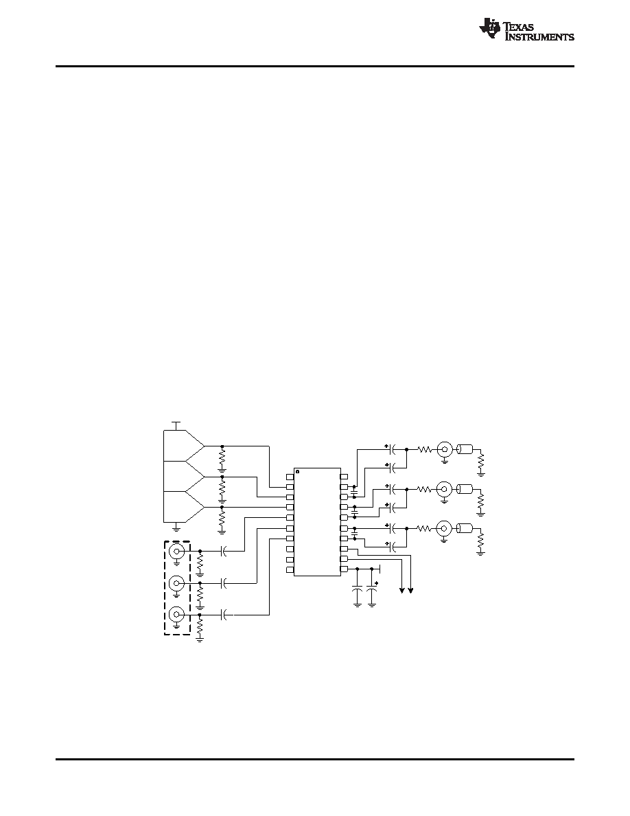
Figure 67 shows a SAG-corrected configuration for the THS7303. If a S-Video chroma channel is being
configured, there is no reason for SAG correction because the coupling capacitor is typically small at 0.1
μF.
Thus, tying the output pin directly to the SAG output pin is recommended along with a 0.1-
μF capacitor.
Note that increasing the gain of the THS7303 can be easilly accomplished by using the SAG pin. Simply placing
a resistor, RSAG, between the SAG pin and GND increases the gain by forming a resistor divider on the signal
feedback path. The resulting gain becomes VOUT/VIN = 2.553 + (1268 / (150 + RSAG)).
A.
If the SAG correction capacitors are more than 15 mm from the THS7313, add a 0.01
μF capacitor as shown.
Figure 67. Typical Y
'P'BP'R System Driving SAG Corrected AC-Coupled Video Lines
32
Copyright
2005–2011, Texas Instruments Incorporated
Product Folder Link(s): THS7303
相关PDF资料 |
PDF描述 |
|---|---|
| THS7303PWG4 | 3 CHANNEL, VIDEO AMPLIFIER, PDSO20 |
| THS7303PWRG4 | 3 CHANNEL, VIDEO AMPLIFIER, PDSO20 |
| THS7315DR | 3 CHANNEL, VIDEO AMPLIFIER, PDSO8 |
| THS7315D | 3 CHANNEL, VIDEO AMPLIFIER, PDSO8 |
| THS7315DG4 | 3 CHANNEL, VIDEO AMPLIFIER, PDSO8 |
相关代理商/技术参数 |
参数描述 |
|---|---|
| THS7303PWG4 | 功能描述:视频放大器 3-Ch Low Power Video RoHS:否 制造商:ON Semiconductor 通道数量:4 电源类型: 工作电源电压:3.3 V, 5 V 电源电流: 最小工作温度: 最大工作温度: 封装 / 箱体:TSSOP-14 封装:Reel |
| THS7303PWR | 功能描述:视频放大器 3-Ch Low Power Video RoHS:否 制造商:ON Semiconductor 通道数量:4 电源类型: 工作电源电压:3.3 V, 5 V 电源电流: 最小工作温度: 最大工作温度: 封装 / 箱体:TSSOP-14 封装:Reel |
| THS7303PWRG4 | 功能描述:视频放大器 3-Ch Low Power Video RoHS:否 制造商:ON Semiconductor 通道数量:4 电源类型: 工作电源电压:3.3 V, 5 V 电源电流: 最小工作温度: 最大工作温度: 封装 / 箱体:TSSOP-14 封装:Reel |
| THS730A A2 | 制造商:Tektronix Inc 功能描述:OSCILLOSCOPE DSO/DMM 200MHZ |
发布紧急采购,3分钟左右您将得到回复。