- 您现在的位置:买卖IC网 > PDF目录98228 > THS7303PW (TEXAS INSTRUMENTS INC) 3 CHANNEL, VIDEO AMPLIFIER, PDSO20 PDF资料下载
参数资料
| 型号: | THS7303PW |
| 厂商: | TEXAS INSTRUMENTS INC |
| 元件分类: | 音频/视频放大 |
| 英文描述: | 3 CHANNEL, VIDEO AMPLIFIER, PDSO20 |
| 封装: | GREEN, PLASTIC, TSSOP-20 |
| 文件页数: | 56/60页 |
| 文件大小: | 1980K |
| 代理商: | THS7303PW |
第1页第2页第3页第4页第5页第6页第7页第8页第9页第10页第11页第12页第13页第14页第15页第16页第17页第18页第19页第20页第21页第22页第23页第24页第25页第26页第27页第28页第29页第30页第31页第32页第33页第34页第35页第36页第37页第38页第39页第40页第41页第42页第43页第44页第45页第46页第47页第48页第49页第50页第51页第52页第53页第54页第55页当前第56页第57页第58页第59页第60页
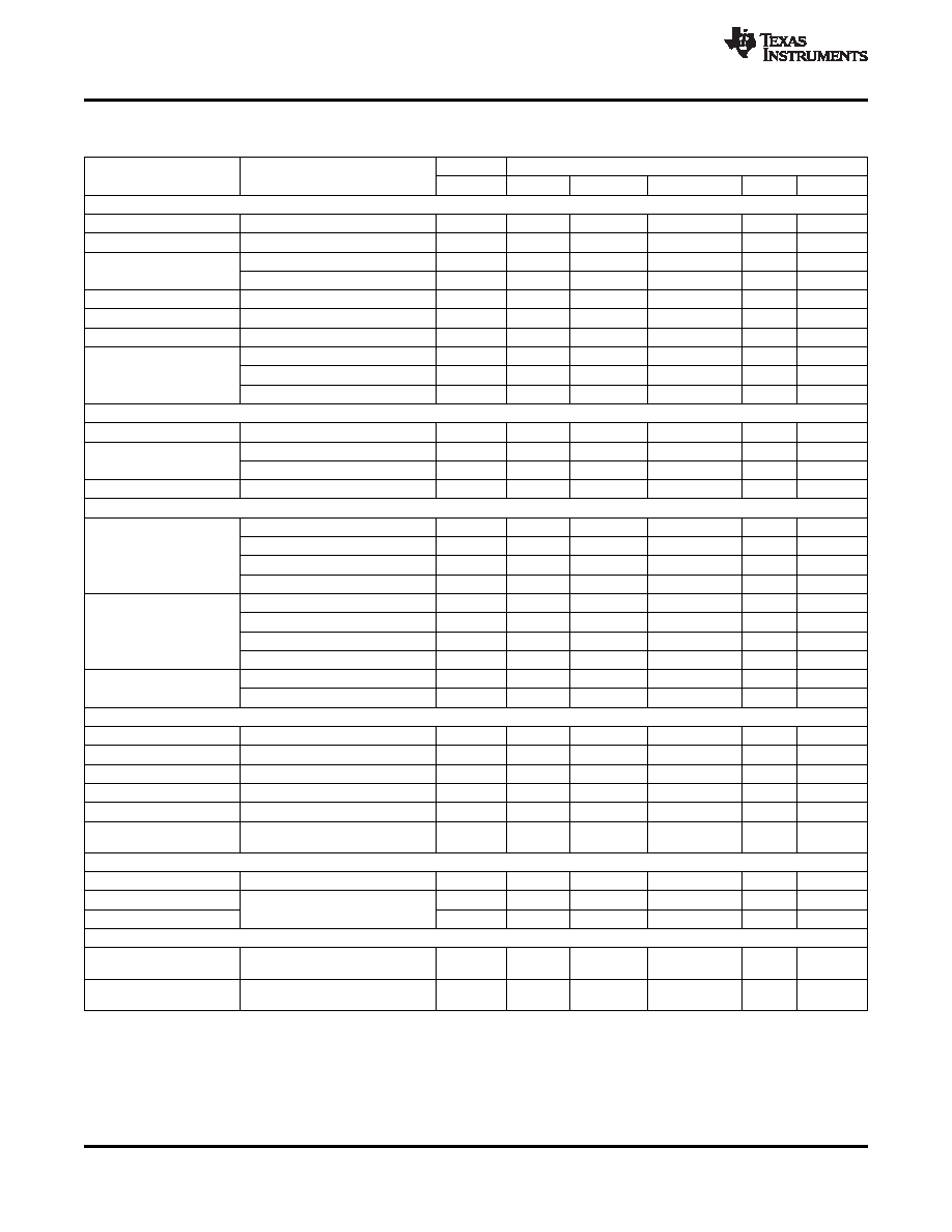
SLOS479B
– OCTOBER 2005 – REVISED MARCH 2011
ELECTRICAL CHARACTERISTICS: VS+ = 5 V (continued)
RL = 150 to GND, filter select = 9 MHz, input bias = dc, and SAG pin shorted to the output pin (unless otherwise noted).
TYP
OVER TEMPERATURE
PARAMETER
TEST CONDITIONS
+25
°C
+25
°C
0
°C to +70°C
–40°C to +85°C
UNITS
MIN/MAX
DC PERFORMANCE
Output offset voltage
Bias = dc
30
90
95
mV
Max
Average offset voltage drift
Bias = dc
20
μV/°C
Bias = dc + 135 mV, VI = 0 V
290
235/345
215/360
200/375
mV
Min/Max
Bias output voltage
Bias = ac
2.5
2.3/2.7
2.25/2.75
V
Min/Max
Sync-tip-clamp output voltage
Bias = ac STC
300
230/375
215/385
210/390
mV
Min/Max
Input bias current
Bias = dc, implies IB out of the pin
–0.6
–4
–5
μA
Max
Average bias current drift
Bias = dc
10
nA/
°C
Bias = ac STC, low bias
1.9
0.6/3.3
0.5/3.5
0.4/3.6
μA
Min/Max
Sync-tip-clamp bias current
Bias = ac STC, mid bias
6
4.3/8.2
4.1/8.4
4/8.5
μA
Min/Max
Bias = ac STC, high bias
8.2
6.2/10.8
6/11
5.9/11.1
μA
Min/Max
INPUT CHARACTERISTICS
Input voltage range
Bias = dc, limited by output
0/2.4
0/2.35
0/2.3
V
Min/Max
Bias = ac bias mode
19
k
Input resistance
Bias = dc, dc + 135 mV, ac STC
3
M
Input capacitance
2
pF
OUTPUT CHARACTERISTICS
RL = 150 to +2.5V
4.8
4.4
4.3
V
Min
RL = 150 to GND
4.65
4.2
4.1
V
Min
High output voltage swing
RL = 75 to +2.5V
4.7
4.3
4.2
V
Min
RL = 75 to GND
4.4
4.1
4
V
Min
RL = 150 to +2.5V
0.2
0.34
0.37
V
Max
RL = 150 to GND
0.1
0.23
0.26
0.27
V
Max
Low output voltage swing
RL = 75 to GND
0.35
0.46
0.5
V
Max
RL = 75 to GND
0.1
0.23
0.26
0.27
V
Max
RL = 10 to +2.5V, sourcing
85
60
57
55
mA
Min
Output current
RL = 10 to +2.5V, sinking
85
60
57
55
mA
Min
POWER SUPPLY
Maximum operating voltage
5
5.5
V
Max
Minimum operating voltage
5
2.6
V
Min
Maximum quiescent current
Per channel VI = 200 mV
6.6
7.9
8.1
8.2
mA
Max
Minimum quiescent current
Per channel VI = 200 mV
6.6
5.3
5.1
5
mA
Min
Total quiescent current
All channels on, VI = 200 mV
(3)
18.9
mA
Power-supply rejection
VS+ = 5.2 V to 4.8 V
66
38
36
dB
Min
(+PSRR)
DISABLE CHARACTERISTICS
Quiescent current
All 3 channels disabled (4)
0.5
μA
Turn-on time delay (tON)
Time reaches 50% of final value after
5
μs
I2C control is completed
Turn-on time delay (tOFF)
2
μs
DIGITAL CHARACTERISTICS
High-level input voltage xxx
3.5
V
Typ
VIH
Low-level input voltage xx x
1.5
V
Typ
VIL
(3)
Due to sharing of internal bias circuitry, the quiescent current (with all channels operating) is less than the single individual channel
quiescent currents added together.
(4)
Note that the I2C circuitry is still active while in Disable mode. The current shown is while there is no activity with the device I2C circuitry.
6
Copyright
2005–2011, Texas Instruments Incorporated
Product Folder Link(s): THS7303
相关PDF资料 |
PDF描述 |
|---|---|
| THS7303PWG4 | 3 CHANNEL, VIDEO AMPLIFIER, PDSO20 |
| THS7303PWRG4 | 3 CHANNEL, VIDEO AMPLIFIER, PDSO20 |
| THS7315DR | 3 CHANNEL, VIDEO AMPLIFIER, PDSO8 |
| THS7315D | 3 CHANNEL, VIDEO AMPLIFIER, PDSO8 |
| THS7315DG4 | 3 CHANNEL, VIDEO AMPLIFIER, PDSO8 |
相关代理商/技术参数 |
参数描述 |
|---|---|
| THS7303PWG4 | 功能描述:视频放大器 3-Ch Low Power Video RoHS:否 制造商:ON Semiconductor 通道数量:4 电源类型: 工作电源电压:3.3 V, 5 V 电源电流: 最小工作温度: 最大工作温度: 封装 / 箱体:TSSOP-14 封装:Reel |
| THS7303PWR | 功能描述:视频放大器 3-Ch Low Power Video RoHS:否 制造商:ON Semiconductor 通道数量:4 电源类型: 工作电源电压:3.3 V, 5 V 电源电流: 最小工作温度: 最大工作温度: 封装 / 箱体:TSSOP-14 封装:Reel |
| THS7303PWRG4 | 功能描述:视频放大器 3-Ch Low Power Video RoHS:否 制造商:ON Semiconductor 通道数量:4 电源类型: 工作电源电压:3.3 V, 5 V 电源电流: 最小工作温度: 最大工作温度: 封装 / 箱体:TSSOP-14 封装:Reel |
| THS730A A2 | 制造商:Tektronix Inc 功能描述:OSCILLOSCOPE DSO/DMM 200MHZ |
发布紧急采购,3分钟左右您将得到回复。