- 您现在的位置:买卖IC网 > PDF目录98229 > THS7365IPW (TEXAS INSTRUMENTS INC) 6 CHANNEL, VIDEO AMPLIFIER, PDSO20 PDF资料下载
参数资料
| 型号: | THS7365IPW |
| 厂商: | TEXAS INSTRUMENTS INC |
| 元件分类: | 音频/视频放大 |
| 英文描述: | 6 CHANNEL, VIDEO AMPLIFIER, PDSO20 |
| 封装: | PLASTIC, TSSOP-20 |
| 文件页数: | 26/52页 |
| 文件大小: | 1599K |
| 代理商: | THS7365IPW |
第1页第2页第3页第4页第5页第6页第7页第8页第9页第10页第11页第12页第13页第14页第15页第16页第17页第18页第19页第20页第21页第22页第23页第24页第25页当前第26页第27页第28页第29页第30页第31页第32页第33页第34页第35页第36页第37页第38页第39页第40页第41页第42页第43页第44页第45页第46页第47页第48页第49页第50页第51页第52页
APPLICATION INFORMATION
INPUT VOLTAGE
INPUT OVERVOLTAGE PROTECTION
+V
S
External
Input/Output
Pin
Internal
Circuitry
OPERATING VOLTAGE
SBOS467 – MARCH 2009.................................................................................................................................................................................................. www.ti.com
allows
operation
down
to
2.6
V,
but
it
is
The THS7365 is targeted for six-channel video output
recommended to use at least a 3-V supply to ensure
applications that require three standard-definition
that no issues arise with headroom or clipping with
(SD) video output buffers and three high-definition
100% color-saturated CVBS signals. If only 75% color
(HD) output buffers. Although it can be used for
saturated CVBS is supported, then the output voltage
numerous
other
applications,
the
needs
and
requirements are reduced to 2 VPP on the output,
requirements of the video signal are the most
allowing a 2.7-V supply to be utilized without issues.
important design parameters of the THS7365. Built
on
the
revolutionary,
complementary
Silicon
A 0.1-
F to 0.01-F capacitor should be placed as
Germanium (SiGe) BiCom3X process, the THS7365
close as possible to the power-supply pins. Failure to
incorporates many features not typically found in
do so may result in the THS7365 outputs ringing or
integrated video parts while consuming very low
oscillating. Additionally, a large capacitor (such as
power. The THS7365 includes the following features:
22
F to 100 F) should be placed on the
power-supply
line
to
minimize
interference
with
Single-supply 2.7-V to 5-V operation with low total
50-/60-Hz line frequencies.
quiescent current of 20.7 mA at 3.3 V and 21.6
mA at 5 V
Disable mode allows for shutting down individual
SD/HD blocks of amplifiers to save system power
The THS7365 input range allows for an input signal
in power-sensitive applications
range from –0.2 V to approximately (VS+ – 1.5 V).
However, because of the internal fixed gain of 2 V/V
Input configuration accepting dc + level shift, ac
(+6 dB) and the internal input level shift of 150 mV
sync-tip clamp, or ac-bias
(typical), the output is generally the limiting factor for
–
AC-biasing is allowed with the use of external
the allowable linear input range. For example, with a
pull-up resistors to the positive power supply
5-V supply, the linear input range is from –0.2 V to
Sixth-order, low-pass filter for DAC reconstruction
3.5 V. However, because of the gain and level shift,
or ADC image rejection:
the linear output range limits the allowable linear
–
9.5 MHz for NTSC, PAL, SECAM, composite
input range to approximately –0.1 V to 2.3 V.
video
(CVBS),
S-Video
Y’/C’,
480i/576i,
Y’/P’B/P’R, and G’B’R’ (R’G’B’) signals
–
36 MHz for 720p, 1080i, or up to 1080p30
The THS7365 is built using a very high-speed,
Y’/P’B/P’R or G’B’R’ signals; also allows up to
complementary, bipolar, and CMOS process. The
XGA (1024 × 768 at 60 Hz) R'G'B' video
internal junction breakdown voltages are relatively
Individually-controlled Bypass mode bypasses the
low for these very small geometry devices. These
low-pass filters for each SD/HD block of amplifiers
breakdowns are reflected in the Absolute Maximum
–
SD bypass mode features 130-MHz and
Ratings table. All input and output device pins are
100-V/
s performance
protected with internal ESD protection diodes to the
–
HD bypass mode features 250-MHz and
power supplies, as shown in Figure 115.
500-V/
s performance
Individually-controlled Disable mode shuts down
all amplifiers in each SD/HD block to reduce
quiescent current to less than 1
A
Internally-fixed gain of 2-V/V (+6-dB) buffer that
can drive two video lines with dc-coupling or
traditional ac-coupling
Flow-through configuration using a TSSOP-20
package that complies with the latest lead-free
(RoHS-compatible)
and
green
manufacturing
requirements
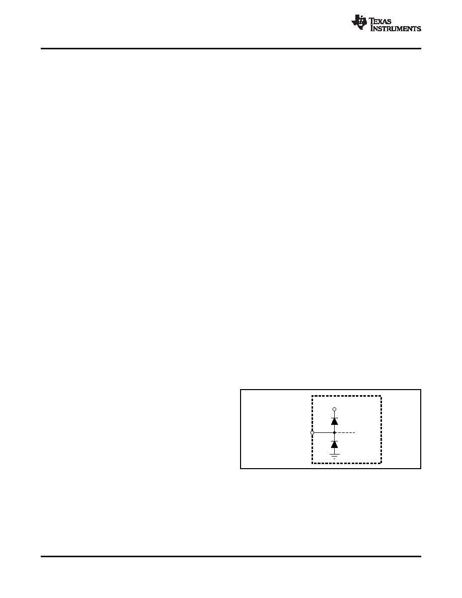
Figure 115. Internal ESD Protection
These diodes provide moderate protection to input
The THS7365 is designed to operate from 2.7 V to
overdrive voltages above and below the supplies as
5 V over a –40°C to +85°C temperature range. The
well. The protection diodes can typically support
impact on performance over the entire temperature
30 mA of continuous current when overdriven.
range is negligible as a result of the implementation
of thin film resistors and high-quality, low-temperature
coefficient capacitors. The design of the THS7365
32
Copyright 2009, Texas Instruments Incorporated
Product Folder Link(s): THS7365
相关PDF资料 |
PDF描述 |
|---|---|
| THS7368IPWR | 6 CHANNEL, VIDEO AMPLIFIER, PDSO20 |
| THS7368IPW | 6 CHANNEL, VIDEO AMPLIFIER, PDSO20 |
| THS7372IPWR | 4 CHANNEL, VIDEO AMPLIFIER, PDSO14 |
| THS7372IPW | 4 CHANNEL, VIDEO AMPLIFIER, PDSO14 |
| THS7374IPWR | 4 CHANNEL, VIDEO AMPLIFIER, PDSO14 |
相关代理商/技术参数 |
参数描述 |
|---|---|
| THS7365IPWR | 功能描述:视频放大器 6Ch Video Amp RoHS:否 制造商:ON Semiconductor 通道数量:4 电源类型: 工作电源电压:3.3 V, 5 V 电源电流: 最小工作温度: 最大工作温度: 封装 / 箱体:TSSOP-14 封装:Reel |
| THS7368 | 制造商:TI 制造商全称:Texas Instruments 功能描述:6-Channel Video Amplifier with 3-SD and 3-SD/ED/HD/Full-HD Filters and 6-dB Gain |
| THS7368EVM | 功能描述:放大器 IC 开发工具 THS7368EVM Eval Mod RoHS:否 制造商:International Rectifier 产品:Demonstration Boards 类型:Power Amplifiers 工具用于评估:IR4302 工作电源电压:13 V to 23 V |
| THS7368IPW | 功能描述:视频放大器 6-Ch Video Amp RoHS:否 制造商:ON Semiconductor 通道数量:4 电源类型: 工作电源电压:3.3 V, 5 V 电源电流: 最小工作温度: 最大工作温度: 封装 / 箱体:TSSOP-14 封装:Reel |
| THS7368IPW | 制造商:Texas Instruments 功能描述:Video Amplifier IC 制造商:Texas Instruments 功能描述:IC, VIDEO AMPLIFIER, HEX, 350MHZ TSSOP20 |
发布紧急采购,3分钟左右您将得到回复。