- 您现在的位置:买卖IC网 > PDF目录98229 > THS7365IPW (TEXAS INSTRUMENTS INC) 6 CHANNEL, VIDEO AMPLIFIER, PDSO20 PDF资料下载
参数资料
| 型号: | THS7365IPW |
| 厂商: | TEXAS INSTRUMENTS INC |
| 元件分类: | 音频/视频放大 |
| 英文描述: | 6 CHANNEL, VIDEO AMPLIFIER, PDSO20 |
| 封装: | PLASTIC, TSSOP-20 |
| 文件页数: | 29/52页 |
| 文件大小: | 1599K |
| 代理商: | THS7365IPW |
第1页第2页第3页第4页第5页第6页第7页第8页第9页第10页第11页第12页第13页第14页第15页第16页第17页第18页第19页第20页第21页第22页第23页第24页第25页第26页第27页第28页当前第29页第30页第31页第32页第33页第34页第35页第36页第37页第38页第39页第40页第41页第42页第43页第44页第45页第46页第47页第48页第49页第50页第51页第52页
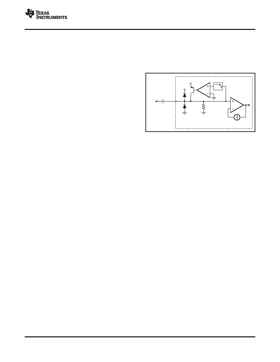
INPUT MODE OF OPERATION: AC SYNC TIP
Level
Shift
Internal
Circuitry
+V
S
800kW
Input
Pin
Input
0.1 mF
g
m
+V
S
STCLPF
www.ti.com.................................................................................................................................................................................................. SBOS467 – MARCH 2009
As a result of this delay, sync may have an apparent
CLAMP
voltage shift. The amount of shift depends on the
amount of droop in the signal as dictated by the input
Some video DACs or encoders are not referenced to
capacitor and the STC current flow. Because sync is
ground but rather to the positive power supply. The
used primarily for timing purposes with syncing
resulting video signals are generally at too great a
occurring on the edge of the sync signal, this shift is
voltage for a dc-coupled video buffer to function
transparent in most systems.
properly. To account for this scenario, the THS7365
incorporates a sync-tip clamp circuit. This function
requires a capacitor (nominally 0.1
F) to be in series
with the input. Although the term sync-tip-clamp is
used throughout this document, it should be noted
that the THS7365 would probably be better termed as
a dc restoration circuit based on how this function is
performed. This circuit is an active clamp circuit and
not a passive diode clamp function.
The input to the THS7365 has an internal control loop
that sets the lowest input applied voltage to clamp at
ground (0 V). By setting the reference at 0 V, the
THS7365 allows a dc-coupled input to also function.
Figure 118. Equivalent AC Sync-Tip-Clamp Input
Therefore, the sync-tip-clamp (STC) is considered
Circuit
transparent because it does not operate unless the
input signal goes below ground. The signal then goes
through the same 150-mV level shifter, resulting in an
While this feature may not fully eliminate overshoot
output voltage low level of 300 mV. If the input signal
issues on the input signal, in cases of extreme
tries to go below 0 V, the THS7365 internal control
overshoot and/or ringing, the STC system should help
loop sources up to 6 mA of current to increase the
minimize improper clamping levels. As an additional
input voltage level on the THS7365 input side of the
method to help minimize this issue, an external
coupling capacitor. As soon as the voltage goes
capacitor (for example, 10 pF to 47 pF) to ground in
above the 0-V level, the loop stops sourcing current
parallel with the external termination resistors can
and becomes very high impedance.
help filter overshoot problems.
One of the concerns about the sync-tip-clamp level is
It should be noted that this STC system is dynamic
how the clamp reacts to a sync edge that has
and does not rely upon timing in any way. It only
overshoot—common in VCR signals, noise, DAC
depends on the voltage that appears at the input pin
overshoot, or reflections found in poor printed circuit
at any given point in time. The STC filtering helps
board (PCB) layouts. Ideally, the STC should not
minimize
level
shift
problems
associated
with
react to the overshoot voltage of the input signal.
switching noises or very short spikes on the signal
Otherwise, this response could result in clipping on
line. This architecture helps ensure a very robust
the rest of the video signal because it may raise the
STC system.
bias voltage too much.
When the ac STC operation is used, there must also
To help minimize this input signal overshoot problem,
be some finite amount of discharge bias current. As
the control loop in the THS7365 has an internal
previously described, if the input signal goes below
low-pass filter, as shown in Figure 118. This filter
the 0-V clamp level, the internal loop of the THS7365
reduces the response time of the STC circuit. This
sources current to increase the voltage appearing at
delay is a function of how far the voltage is below
the input pin. As the difference between the signal
ground, but in general it is approximately a 400-ns
level and the 0-V reference level increases, the
delay for the 9.5-MHz filters and approximately a
amount
of
source
current
increases
150-ns delay for the 36-MHz filters. The effect of this
proportionally—supplying up to 6 mA of current.
filter is to slow down the response of the control loop
Thus, the time to re-establish the proper STC voltage
so as not to clamp on the input overshoot voltage but
can be very fast. If the difference is very small, then
rather the flat portion of the sync signal.
the source current is also very small to account for
minor voltage droop.
Copyright 2009, Texas Instruments Incorporated
35
Product Folder Link(s): THS7365
相关PDF资料 |
PDF描述 |
|---|---|
| THS7368IPWR | 6 CHANNEL, VIDEO AMPLIFIER, PDSO20 |
| THS7368IPW | 6 CHANNEL, VIDEO AMPLIFIER, PDSO20 |
| THS7372IPWR | 4 CHANNEL, VIDEO AMPLIFIER, PDSO14 |
| THS7372IPW | 4 CHANNEL, VIDEO AMPLIFIER, PDSO14 |
| THS7374IPWR | 4 CHANNEL, VIDEO AMPLIFIER, PDSO14 |
相关代理商/技术参数 |
参数描述 |
|---|---|
| THS7365IPWR | 功能描述:视频放大器 6Ch Video Amp RoHS:否 制造商:ON Semiconductor 通道数量:4 电源类型: 工作电源电压:3.3 V, 5 V 电源电流: 最小工作温度: 最大工作温度: 封装 / 箱体:TSSOP-14 封装:Reel |
| THS7368 | 制造商:TI 制造商全称:Texas Instruments 功能描述:6-Channel Video Amplifier with 3-SD and 3-SD/ED/HD/Full-HD Filters and 6-dB Gain |
| THS7368EVM | 功能描述:放大器 IC 开发工具 THS7368EVM Eval Mod RoHS:否 制造商:International Rectifier 产品:Demonstration Boards 类型:Power Amplifiers 工具用于评估:IR4302 工作电源电压:13 V to 23 V |
| THS7368IPW | 功能描述:视频放大器 6-Ch Video Amp RoHS:否 制造商:ON Semiconductor 通道数量:4 电源类型: 工作电源电压:3.3 V, 5 V 电源电流: 最小工作温度: 最大工作温度: 封装 / 箱体:TSSOP-14 封装:Reel |
| THS7368IPW | 制造商:Texas Instruments 功能描述:Video Amplifier IC 制造商:Texas Instruments 功能描述:IC, VIDEO AMPLIFIER, HEX, 350MHZ TSSOP20 |
发布紧急采购,3分钟左右您将得到回复。