- 您现在的位置:买卖IC网 > PDF目录299979 > TLV2373IDRG4 (TEXAS INSTRUMENTS INC) DUAL OP-AMP, 6000 uV OFFSET-MAX, 3 MHz BAND WIDTH, PDSO14 PDF资料下载
参数资料
| 型号: | TLV2373IDRG4 |
| 厂商: | TEXAS INSTRUMENTS INC |
| 元件分类: | 运算放大器 |
| 英文描述: | DUAL OP-AMP, 6000 uV OFFSET-MAX, 3 MHz BAND WIDTH, PDSO14 |
| 封装: | GREEN, PLASTIC, MS-012AB, SOIC-14 |
| 文件页数: | 6/41页 |
| 文件大小: | 1390K |
| 代理商: | TLV2373IDRG4 |
第1页第2页第3页第4页第5页当前第6页第7页第8页第9页第10页第11页第12页第13页第14页第15页第16页第17页第18页第19页第20页第21页第22页第23页第24页第25页第26页第27页第28页第29页第30页第31页第32页第33页第34页第35页第36页第37页第38页第39页第40页第41页
TLV2370, TLV2371, TLV2372, TLV2373, TLV2374, TLV2375
FAMILY OF 550 A/Ch 3MHz RAILTORAIL INPUT/OUTPUT
OPERATIONAL AMPLIFIERS WITH SHUTDOWN
SLOS270D MARCH 2001 REVISED JANUARY 2005
14
WWW.TI.COM
POST OFFICE BOX 655303
DALLAS, TEXAS 75265
APPLICATION INFORMATION
rail-to-rail input operation
The TLV237x input stage consists of two differential transistor pairs, NMOS and PMOS, that operate together
to achieve rail-to-rail input operation. The transition point between these two pairs can be seen in Figure 1,
Figure 2, and Figure 3 for a 2.7-V, 5-V, and 15-V supply. As the common-mode input voltage approaches the
positive supply rail, the input pair switches from the PMOS differential pair to the NMOS differential pair. This
transition occurs approximately 1.35 V from the positive rail and results in a change in offset voltage due to
different device characteristics between the NMOS and PMOS pairs. If the input signal to the device is large
enough to swing between both rails, this transition results in a reduction in common-mode rejection ratio
(CMRR). If the input signal does not swing between both rails, it is best to bias the signal in the region where
only one input pair is active. This is the region in Figure 1 through Figure 3 where the offset voltage varies slightly
across the input range and optimal CMRR can be achieved. This has the greatest impact when operating from
a 2.7-V supply voltage.
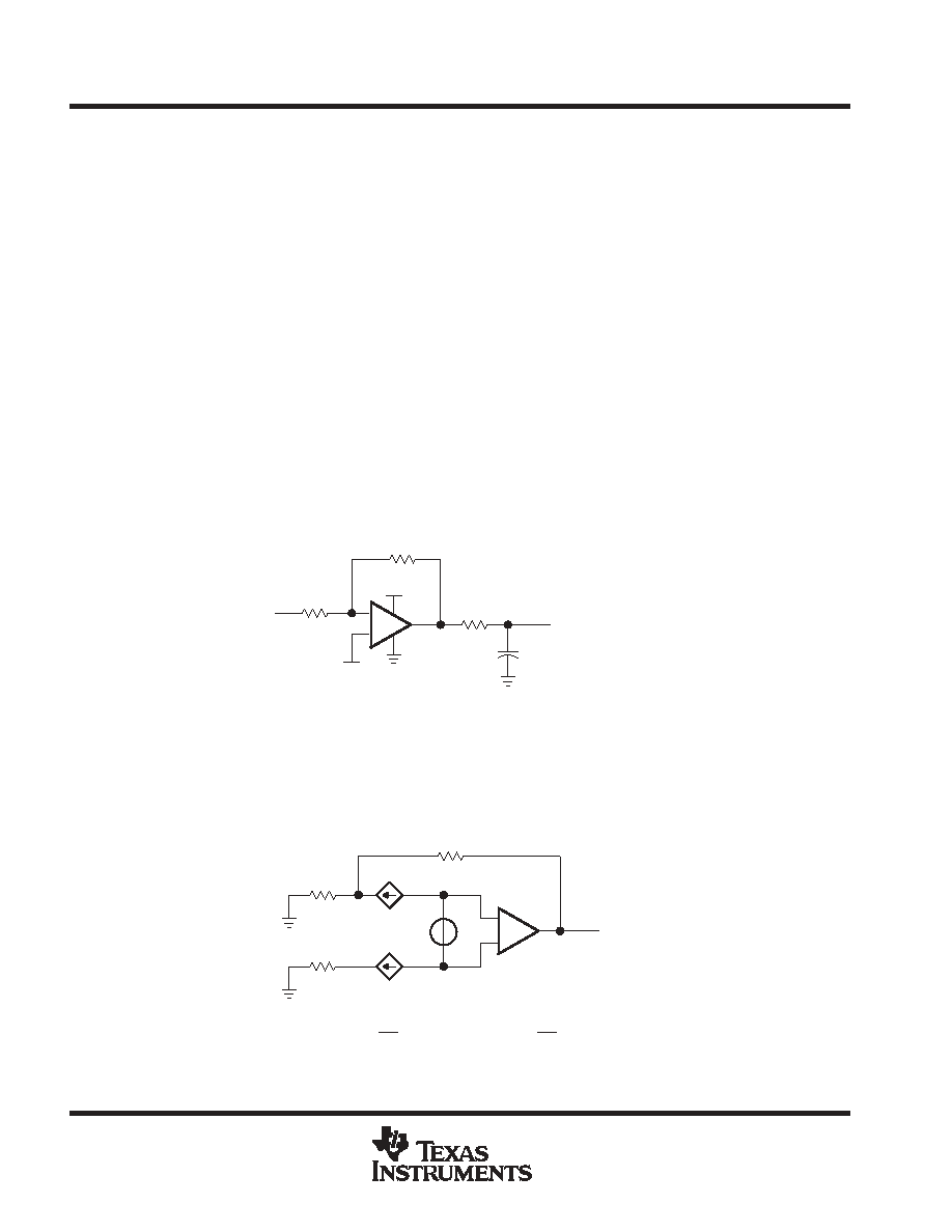
driving a capacitive load
When the amplifier is configured in this manner, capacitive loading directly on the output decreases the device’s
phase margin leading to high frequency ringing or oscillations. Therefore, for capacitive loads of greater than
10 pF, it is recommended that a resistor be placed in series (RNULL) with the output of the amplifier, as shown
in Figure 33. A minimum value of 20
should work well for most applications.
CLOAD
RF
Input
Output
RG
RNULL
+
VDD/2
Figure 33. Driving a Capacitive Load
offset voltage
The output offset voltage, (VOO) is the sum of the input offset voltage (VIO) and both input bias currents (IIB) times
the corresponding gains. The following schematic and formula can be used to calculate the output offset
voltage:
V
OO +
V
IO
1
)
R
F
R
G
" I
IB
)
R
S
1
)
R
F
R
G
" I
IB–
R
F
+
VI
+
RG
RS
RF
IIB
VO
IIB+
Figure 34. Output Offset Voltage Model
相关PDF资料 |
PDF描述 |
|---|---|
| TLV2375IDG4 | QUAD OP-AMP, 6000 uV OFFSET-MAX, 3 MHz BAND WIDTH, PDSO16 |
| TLV2375IPWG4 | QUAD OP-AMP, 6000 uV OFFSET-MAX, 3 MHz BAND WIDTH, PDSO16 |
| TLV2454AINE4 | QUAD OP-AMP, 1300 uV OFFSET-MAX, 0.2 MHz BAND WIDTH, PDIP14 |
| TLV2454CNE4 | QUAD OP-AMP, 2000 uV OFFSET-MAX, 0.2 MHz BAND WIDTH, PDIP14 |
| TLV2454INE4 | QUAD OP-AMP, 2000 uV OFFSET-MAX, 0.2 MHz BAND WIDTH, PDIP14 |
相关代理商/技术参数 |
参数描述 |
|---|---|
| TLV2373IN | 功能描述:运算放大器 - 运放 Dual 3MHz R-R Op Amp RoHS:否 制造商:STMicroelectronics 通道数量:4 共模抑制比(最小值):63 dB 输入补偿电压:1 mV 输入偏流(最大值):10 pA 工作电源电压:2.7 V to 5.5 V 安装风格:SMD/SMT 封装 / 箱体:QFN-16 转换速度:0.89 V/us 关闭:No 输出电流:55 mA 最大工作温度:+ 125 C 封装:Reel |
| TLV2373INE4 | 功能描述:运算放大器 - 运放 550-uA/Ch 3-MHz RRIO Op Amp w/Shutdown RoHS:否 制造商:STMicroelectronics 通道数量:4 共模抑制比(最小值):63 dB 输入补偿电压:1 mV 输入偏流(最大值):10 pA 工作电源电压:2.7 V to 5.5 V 安装风格:SMD/SMT 封装 / 箱体:QFN-16 转换速度:0.89 V/us 关闭:No 输出电流:55 mA 最大工作温度:+ 125 C 封装:Reel |
| TLV2374 | 制造商:TI 制造商全称:Texas Instruments 功能描述:FAMILY OF 550- UA/CH 3-MHz RAIL-TO-RAIL INPUT/OUTPUT OPERATIONAL AMPLIFIERS WITH SHUTDOWN |
| TLV2374ID | 功能描述:运算放大器 - 运放 550-uA/Channel 3-MHz RRIO Op Amp RoHS:否 制造商:STMicroelectronics 通道数量:4 共模抑制比(最小值):63 dB 输入补偿电压:1 mV 输入偏流(最大值):10 pA 工作电源电压:2.7 V to 5.5 V 安装风格:SMD/SMT 封装 / 箱体:QFN-16 转换速度:0.89 V/us 关闭:No 输出电流:55 mA 最大工作温度:+ 125 C 封装:Reel |
| TLV2374IDG4 | 功能描述:运算放大器 - 运放 550-uA/Channel 3-MHz RRIO Op Amp RoHS:否 制造商:STMicroelectronics 通道数量:4 共模抑制比(最小值):63 dB 输入补偿电压:1 mV 输入偏流(最大值):10 pA 工作电源电压:2.7 V to 5.5 V 安装风格:SMD/SMT 封装 / 箱体:QFN-16 转换速度:0.89 V/us 关闭:No 输出电流:55 mA 最大工作温度:+ 125 C 封装:Reel |
发布紧急采购,3分钟左右您将得到回复。