- 您现在的位置:买卖IC网 > PDF目录98252 > TLV2556MPWREPG4 (TEXAS INSTRUMENTS INC) 11-CH 12-BIT SUCCESSIVE APPROXIMATION ADC, SERIAL ACCESS, PDSO20 PDF资料下载
参数资料
| 型号: | TLV2556MPWREPG4 |
| 厂商: | TEXAS INSTRUMENTS INC |
| 元件分类: | ADC |
| 英文描述: | 11-CH 12-BIT SUCCESSIVE APPROXIMATION ADC, SERIAL ACCESS, PDSO20 |
| 封装: | GREEN, PLASTIC, TSSOP-20 |
| 文件页数: | 22/37页 |
| 文件大小: | 705K |
| 代理商: | TLV2556MPWREPG4 |
第1页第2页第3页第4页第5页第6页第7页第8页第9页第10页第11页第12页第13页第14页第15页第16页第17页第18页第19页第20页第21页当前第22页第23页第24页第25页第26页第27页第28页第29页第30页第31页第32页第33页第34页第35页第36页第37页
01: 8-bit output length
X0: 12-bit output length
11: 16-bit output length (default)
0: MSB out first (default)
1: LSB out first
0: Unipolar binary (default)
1: Bipolar 2s complement
00: Internal 4.096 reference
01: Internal 2.048 reference
11: External reference (default)
0: Pin 19 output EOC (default)
1: Pin 19 output Int
0: Normal mode
(CFGR1 needs to be programmed)
1: Default mode enabled
(D[3:0] of CFGR1 and D[3:1] of
CFGR2 set to default)
SDI D[7:4]
Binary,
HEX
COMMAND
0000b
0001b
0010b
0011b
0100b
0101b
0110b
0111b
1000b
1001b
1010b
1011b
1100b
1101b
1110b
1111b
0h
1h
2h
3h
4h
5h
6h
7h
8h
9h
Ah
Bh
Ch
Dh
Eh
Fh
SELECT analog input channel 0
SELECT analog input channel 1
SELECT analog input channel 2
SELECT analog input channel 3
SELECT analog input channel 4
SELECT analog input channel 5
SELECT analog input channel 6
SELECT analog input channel 7
SELECT analog input channel 8
SELECT analog input channel 9
SELECT analog input channel 10
SELECT TEST,
Voltage = (VREF+ + VREF)/2
SELECT TEST, Voltage = REFM
SELECT TEST, Voltage = REFP
SW POWERDOWN (analog + reference)
ACCESS CFGR2
CONFIGURATION
CFGR1
SDI
D[3:0]
D[3:2]
D1
D0
CONFIGURATION
CFGR2
SDI
D[3:0]
D[3:2]
D1
D0
Data Input – Address/Command Bits
Data Output Length
www.ti.com ................................................................................................................................................... SLAS598A – NOVEMBER 2008 – REVISED JULY 2009
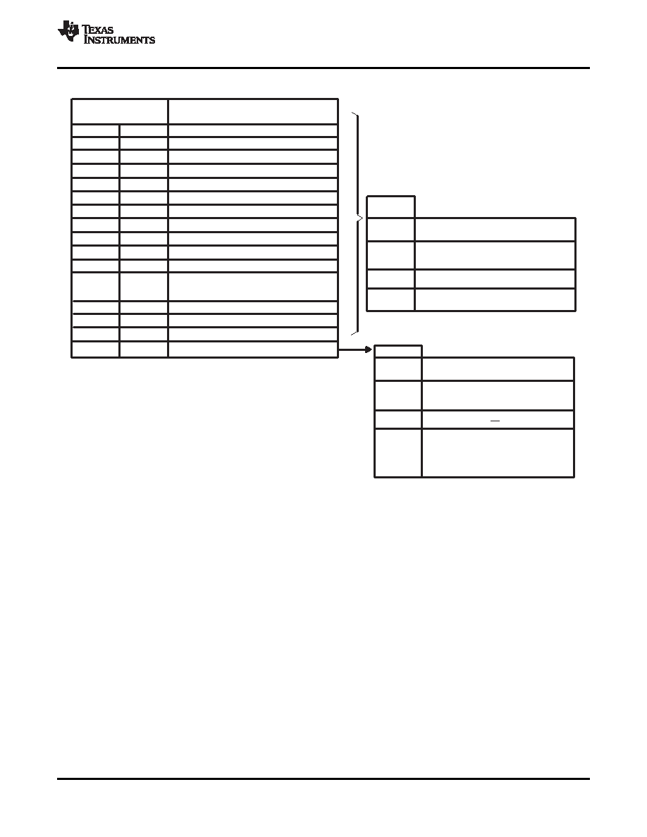
Table 2. Command Set (CMR) and Configuration
The four MSBs (D7–D4) of the input data register are the address or command. These bits can be used to
address one of the 11 input channels, select one of three reference-test voltages, activate the software
power-down mode, or access the second configuration register, CFGR2. All address/command bits affect the
current conversion, which is the conversion that immediately follows the current I/O cycle. They also allow
access to CFGR1 except for command 1111b, which allows access to CFGR2.
CFGR1 bits (D3 and D2) of the data register select the output data length. The data-length selection is valid for
the current I/O cycle (the cycle in which the data is read). The data-length selection, being valid for the current
I/O cycle, allows device start-up without losing I/O synchronization. A data length of 8, 12, or 16 bits can be
selected. Since the converter has 12-bit resolution, a data length of 12 bits is suggested.
With D3 and D2 set to 00 or 10, the device is in the 12-bit data-length mode and the result of the current
conversion is output as a 12-bit serial data stream during the next I/O cycle. The current I/O cycle must be
exactly 12 bits long for proper synchronization, even when this means corrupting the output data from a previous
conversion. The current conversion is started immediately after the twelfth falling edge of the current I/O cycle.
Copyright 2008–2009, Texas Instruments Incorporated
29
Product Folder Link(s): TLV2556-EP
相关PDF资料 |
PDF描述 |
|---|---|
| TLV320ADC3001IYZHT | 2-CH 16-BIT PROPRIETARY METHOD ADC, SERIAL ACCESS, PBGA16 |
| TLV320ADC3001IYZHR | 2-CH 16-BIT PROPRIETARY METHOD ADC, SERIAL ACCESS, PBGA16 |
| TLV320ADC3101IRGER320 | SPECIALTY CONSUMER CIRCUIT, PQCC24 |
| TLV320ADC3101IRGET320 | SPECIALTY CONSUMER CIRCUIT, PQCC24 |
| TLV320ADC3101IRGER | SPECIALTY CONSUMER CIRCUIT, PQCC24 |
相关代理商/技术参数 |
参数描述 |
|---|---|
| TLV2620ID | 制造商:Rochester Electronics LLC 功能描述:- Bulk |
| TLV2620IDBVR | 功能描述:运算放大器 - 运放 800 uA/ch 11MHz RRO Lo-Vltg 1-Ch RoHS:否 制造商:STMicroelectronics 通道数量:4 共模抑制比(最小值):63 dB 输入补偿电压:1 mV 输入偏流(最大值):10 pA 工作电源电压:2.7 V to 5.5 V 安装风格:SMD/SMT 封装 / 箱体:QFN-16 转换速度:0.89 V/us 关闭:No 输出电流:55 mA 最大工作温度:+ 125 C 封装:Reel |
| TLV2620IDBVRG4 | 功能描述:运算放大器 - 运放 800 uA/ch 11MHz RRO Lo-Vltg 1-Ch RoHS:否 制造商:STMicroelectronics 通道数量:4 共模抑制比(最小值):63 dB 输入补偿电压:1 mV 输入偏流(最大值):10 pA 工作电源电压:2.7 V to 5.5 V 安装风格:SMD/SMT 封装 / 箱体:QFN-16 转换速度:0.89 V/us 关闭:No 输出电流:55 mA 最大工作温度:+ 125 C 封装:Reel |
| TLV2620IDBVT | 功能描述:运算放大器 - 运放 800 uA/ch 11MHz RRO Lo-Vltg 1-Ch RoHS:否 制造商:STMicroelectronics 通道数量:4 共模抑制比(最小值):63 dB 输入补偿电压:1 mV 输入偏流(最大值):10 pA 工作电源电压:2.7 V to 5.5 V 安装风格:SMD/SMT 封装 / 箱体:QFN-16 转换速度:0.89 V/us 关闭:No 输出电流:55 mA 最大工作温度:+ 125 C 封装:Reel |
| TLV2620IDBVTG4 | 功能描述:运算放大器 - 运放 800 uA/ch 11MHz RRO Lo-Vltg 1-Ch RoHS:否 制造商:STMicroelectronics 通道数量:4 共模抑制比(最小值):63 dB 输入补偿电压:1 mV 输入偏流(最大值):10 pA 工作电源电压:2.7 V to 5.5 V 安装风格:SMD/SMT 封装 / 箱体:QFN-16 转换速度:0.89 V/us 关闭:No 输出电流:55 mA 最大工作温度:+ 125 C 封装:Reel |
发布紧急采购,3分钟左右您将得到回复。