- 您现在的位置:买卖IC网 > PDF目录98252 > TLV2556MPWREPG4 (TEXAS INSTRUMENTS INC) 11-CH 12-BIT SUCCESSIVE APPROXIMATION ADC, SERIAL ACCESS, PDSO20 PDF资料下载
参数资料
| 型号: | TLV2556MPWREPG4 |
| 厂商: | TEXAS INSTRUMENTS INC |
| 元件分类: | ADC |
| 英文描述: | 11-CH 12-BIT SUCCESSIVE APPROXIMATION ADC, SERIAL ACCESS, PDSO20 |
| 封装: | GREEN, PLASTIC, TSSOP-20 |
| 文件页数: | 25/37页 |
| 文件大小: | 705K |
| 代理商: | TLV2556MPWREPG4 |
第1页第2页第3页第4页第5页第6页第7页第8页第9页第10页第11页第12页第13页第14页第15页第16页第17页第18页第19页第20页第21页第22页第23页第24页当前第25页第26页第27页第28页第29页第30页第31页第32页第33页第34页第35页第36页第37页
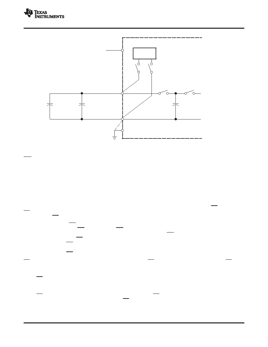
C1
0.1
F
Decoupling Cap
C2
10
F
Int Reference
Compensation Cap
GND
Analog
Supply
Sample
50 pF
CDAC
Convert
REF+
REF
Internal
Reference
VCC
S1, S2:
Closed = Internal Reference Used
Opened = External Reference Used
C2 and Grounding REF Are Required
When Either 4.096 V or 2.048 Internal
Reference Is Used
S1
S2
INT/EOC Output
Chip-Select Input (CS)
www.ti.com ................................................................................................................................................... SLAS598A – NOVEMBER 2008 – REVISED JULY 2009
Figure 54. Reference Block
Pin 19 outputs the status of the ADC conversion. When programmed as EOC, the output indicates the beginning
and the end of conversion. In the reset state, EOC is always high. During the sampling period (beginning after
the fourth falling edge of the I/O CLOCK sequence), EOC remains high until the internal sampling switch of the
converter is safely opened. The opening of the sampling switch occurs after the eighth, twelfth, or sixteenth I/O
CLOCK falling edge, depending on the data-length selection in the input data register. After the EOC signal goes
low, the analog input signal can be changed without affecting the conversion result.
The EOC signal goes high again after the conversion is completed and the conversion result is latched into the
output data register. The rising edge of EOC returns the converter to a reset state and a new I/O cycle begins.
On the rising edge of EOC, the first bit of the current conversion result is on DATA OUT when CS is low. When
CS is toggled between conversions, the first bit of the current conversion result occurs on DATA OUT at the
falling edge of CS.
When programmed as INT, the output indicates that the conversion is completed and the output data is ready to
be read. In the reset state, INT is always high. INT is high during the sampling period and until the conversion is
complete. After the conversion is finished and the output data is latched, INT goes low and remains low until it is
cleared by the host. When CS is held low, the MSB (or LSB) of the conversion result is presented on DATA OUT
on the falling edge of INT. A rising I/O CLOCK edge clears the interrupt.
CS enables and disables the device. During normal operation, CS should be low. Although the use of CS is not
necessary to synchronize a data transfer, it can be brought high between conversions to coordinate the data
transfer of several devices sharing the same bus.
When CS is brought high, the serial-data output is immediately brought to the high-impedance state, releasing its
output data line to other devices that may share it. After an internally generated debounce time, I/O CLOCK is
inhibited, thus preventing any further change in the internal state.
When CS is subsequently brought low again, the device is reset. CS must be held low for an internal debounce
time before the reset operation takes effect. After CS is debounced low, I/O CLOCK must remain inactive (low)
for a minimum time before a new I/O cycle can start.
Copyright 2008–2009, Texas Instruments Incorporated
31
Product Folder Link(s): TLV2556-EP
相关PDF资料 |
PDF描述 |
|---|---|
| TLV320ADC3001IYZHT | 2-CH 16-BIT PROPRIETARY METHOD ADC, SERIAL ACCESS, PBGA16 |
| TLV320ADC3001IYZHR | 2-CH 16-BIT PROPRIETARY METHOD ADC, SERIAL ACCESS, PBGA16 |
| TLV320ADC3101IRGER320 | SPECIALTY CONSUMER CIRCUIT, PQCC24 |
| TLV320ADC3101IRGET320 | SPECIALTY CONSUMER CIRCUIT, PQCC24 |
| TLV320ADC3101IRGER | SPECIALTY CONSUMER CIRCUIT, PQCC24 |
相关代理商/技术参数 |
参数描述 |
|---|---|
| TLV2620ID | 制造商:Rochester Electronics LLC 功能描述:- Bulk |
| TLV2620IDBVR | 功能描述:运算放大器 - 运放 800 uA/ch 11MHz RRO Lo-Vltg 1-Ch RoHS:否 制造商:STMicroelectronics 通道数量:4 共模抑制比(最小值):63 dB 输入补偿电压:1 mV 输入偏流(最大值):10 pA 工作电源电压:2.7 V to 5.5 V 安装风格:SMD/SMT 封装 / 箱体:QFN-16 转换速度:0.89 V/us 关闭:No 输出电流:55 mA 最大工作温度:+ 125 C 封装:Reel |
| TLV2620IDBVRG4 | 功能描述:运算放大器 - 运放 800 uA/ch 11MHz RRO Lo-Vltg 1-Ch RoHS:否 制造商:STMicroelectronics 通道数量:4 共模抑制比(最小值):63 dB 输入补偿电压:1 mV 输入偏流(最大值):10 pA 工作电源电压:2.7 V to 5.5 V 安装风格:SMD/SMT 封装 / 箱体:QFN-16 转换速度:0.89 V/us 关闭:No 输出电流:55 mA 最大工作温度:+ 125 C 封装:Reel |
| TLV2620IDBVT | 功能描述:运算放大器 - 运放 800 uA/ch 11MHz RRO Lo-Vltg 1-Ch RoHS:否 制造商:STMicroelectronics 通道数量:4 共模抑制比(最小值):63 dB 输入补偿电压:1 mV 输入偏流(最大值):10 pA 工作电源电压:2.7 V to 5.5 V 安装风格:SMD/SMT 封装 / 箱体:QFN-16 转换速度:0.89 V/us 关闭:No 输出电流:55 mA 最大工作温度:+ 125 C 封装:Reel |
| TLV2620IDBVTG4 | 功能描述:运算放大器 - 运放 800 uA/ch 11MHz RRO Lo-Vltg 1-Ch RoHS:否 制造商:STMicroelectronics 通道数量:4 共模抑制比(最小值):63 dB 输入补偿电压:1 mV 输入偏流(最大值):10 pA 工作电源电压:2.7 V to 5.5 V 安装风格:SMD/SMT 封装 / 箱体:QFN-16 转换速度:0.89 V/us 关闭:No 输出电流:55 mA 最大工作温度:+ 125 C 封装:Reel |
发布紧急采购,3分钟左右您将得到回复。