- 您现在的位置:买卖IC网 > PDF目录98252 > TLV320ADC3101IRGER (TEXAS INSTRUMENTS INC) SPECIALTY CONSUMER CIRCUIT, PQCC24 PDF资料下载
参数资料
| 型号: | TLV320ADC3101IRGER |
| 厂商: | TEXAS INSTRUMENTS INC |
| 元件分类: | 消费家电 |
| 英文描述: | SPECIALTY CONSUMER CIRCUIT, PQCC24 |
| 封装: | GREEN, PLASTIC, VQFN-24 |
| 文件页数: | 13/84页 |
| 文件大小: | 1363K |
| 代理商: | TLV320ADC3101IRGER |
第1页第2页第3页第4页第5页第6页第7页第8页第9页第10页第11页第12页当前第13页第14页第15页第16页第17页第18页第19页第20页第21页第22页第23页第24页第25页第26页第27页第28页第29页第30页第31页第32页第33页第34页第35页第36页第37页第38页第39页第40页第41页第42页第43页第44页第45页第46页第47页第48页第49页第50页第51页第52页第53页第54页第55页第56页第57页第58页第59页第60页第61页第62页第63页第64页第65页第66页第67页第68页第69页第70页第71页第72页第73页第74页第75页第76页第77页第78页第79页第80页第81页第82页第83页第84页
LD (n)
LD(n+1)
2
1
0
3
2
1
0
3
RD (n)
WORD
CLOCK
BIT
CLOCK
DATA
n-1 n-2 n-3
Left Channel
Right Channel
Ch_Offset_1 = 0
Ch_Offset_2 = 1
RD(n)
RD(n+1)
2
1
0
3
2
1
0
3
LD (n)
WORD
CLOCK
BIT
CLOCK
DATA
n-1 n-2 n-3
Right Channel
Left Channel
Ch_Offset_1 = 0
Ch_Offset_2 = 1
I2S Mode
SLAS553A – NOVEMBER 2008 – REVISED SEPTEMBER 2009...................................................................................................................................... www.ti.com
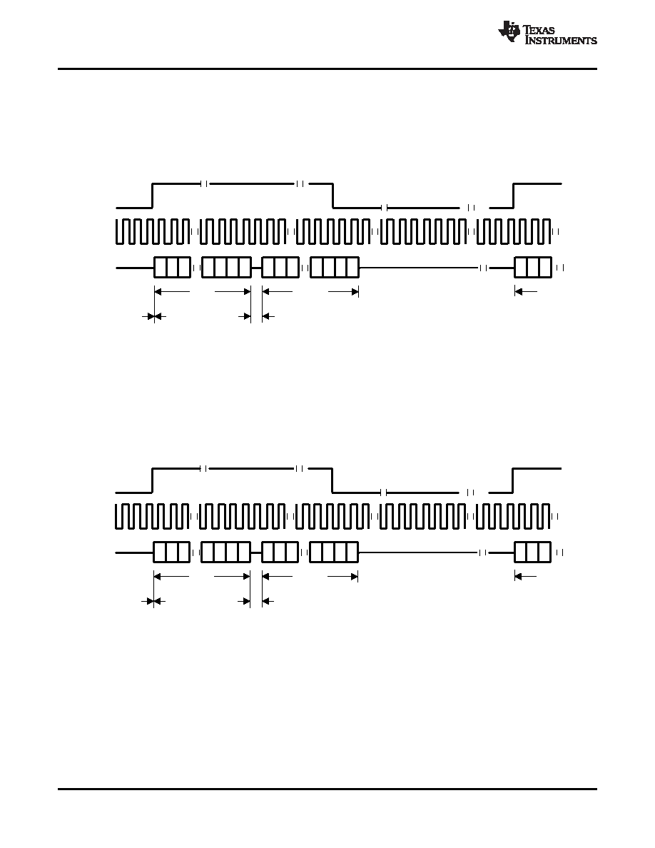
When time-based-slot mode is enabled with no channel swapping, the MSB of the left channel is valid on the
(Offset1 + 1)th rising edge of the bit clock following the rising edge of the word clock. And, the MSB of the right
channel is valid on the (Ch_Offset_2 + 1)th rising edge of the bit clock following the LSB of the left channel.
Figure 21 shows the operation with time-based-slot mode enabled and Ch_Offset_1 = 0 and Ch_Offset_2 = 1.
The MSB of the left channel is valid on the first rising edge of the bit clock after the rising edge of the word clock.
Data transfer for the right channel does not wait for the falling edge of the word clock, and the MSB of the right
channel is valid on the second rising edge of the bit clock after the LSB of the left channel.
Figure 21. Left-Justified Mode, Time-Based-Slot Mode Enabled, Ch_Offset_1 = 0, Ch_Offset_2 = 1
For the case with time-based-slot mode enabled and channel swapping enabled, the MSB of the right channel is
valid on the (Ch_Offset_1 + 1)th rising edge of the bit clock following the rising edge of the word clock. And, the
MSB of the left channel is valid on the (Ch_Offset_2 + 1)th rising edge of the bit clock following the LSB of the
right channel. Figure 22 shows the operation in this mode with Ch_Offset_1 = 0 and Ch_Offset_2 = 1. The MSB
of the right channel is valid on the first rising edge of the bit clock after the rising edge of the word clock. Data
transfer for the left channel starts following the completion of data transfer for the right channel without waiting for
the falling edge of the word clock. The MSB of the left channel is valid on the second rising edge of the bit clock
after the LSB of the right channel.
Figure 22. Left-Justified Mode, Time-Based-Slot Mode Enabled, Ch_Offset_1 = 0, Ch_Offset_2 = 1,
Channel Swapping Enabled
In I2S mode, the MSB of the left channel is valid on the second rising edge of the bit clock after the falling edge
of the word clock. Similarly, the MSB of the right channel is valid on the second rising edge of the bit clock after
20
Copyright 2008–2009, Texas Instruments Incorporated
Product Folder Link(s) :TLV320ADC3101
相关PDF资料 |
PDF描述 |
|---|---|
| TLV320ADC3101IRGET | SPECIALTY CONSUMER CIRCUIT, PQCC24 |
| TLV320AIC10C | SPECIALTY CONSUMER CIRCUIT, PQFP48 |
| TLV320AIC10I | SPECIALTY CONSUMER CIRCUIT, PQFP48 |
| TLV320AIC10CPFB | SPECIALTY CONSUMER CIRCUIT, PQFP48 |
| TLV320AIC10IPFB | SPECIALTY CONSUMER CIRCUIT, PQFP48 |
相关代理商/技术参数 |
参数描述 |
|---|---|
| TLV320ADC3101IRGET | 功能描述:音频模/数转换器 IC 92dB (16B) Low Power Stereo ADC RoHS:否 制造商:Wolfson Microelectronics 转换速率: 分辨率: ADC 输入端数量: 工作电源电压: 最大工作温度: 最小工作温度: 安装风格: 封装 / 箱体: 封装: |
| TLV320AIC10 | 制造商:TI 制造商全称:Texas Instruments 功能描述:General-Purpose 3V to 5.5V 16-bit 22-KSPS DSP CODEC |
| TLV320AIC10C | 制造商:TI 制造商全称:Texas Instruments 功能描述:General-Purpose 3V to 5.5V 16-bit 22-KSPS DSP CODEC |
| TLV320AIC10CGQER | 功能描述:接口—CODEC 16-Bit 22-KSPS DSP Codec RoHS:否 制造商:Texas Instruments 类型: 分辨率: 转换速率:48 kSPs 接口类型:I2C ADC 数量:2 DAC 数量:4 工作电源电压:1.8 V, 2.1 V, 2.3 V to 5.5 V 最大工作温度:+ 85 C 安装风格:SMD/SMT 封装 / 箱体:DSBGA-81 封装:Reel |
| TLV320AIC10CPFB | 功能描述:接口—CODEC 16-Bit 22-KSPS DSP Codec RoHS:否 制造商:Texas Instruments 类型: 分辨率: 转换速率:48 kSPs 接口类型:I2C ADC 数量:2 DAC 数量:4 工作电源电压:1.8 V, 2.1 V, 2.3 V to 5.5 V 最大工作温度:+ 85 C 安装风格:SMD/SMT 封装 / 箱体:DSBGA-81 封装:Reel |
发布紧急采购,3分钟左右您将得到回复。