- 您现在的位置:买卖IC网 > PDF目录98252 > TLV320ADC3101IRGER (TEXAS INSTRUMENTS INC) SPECIALTY CONSUMER CIRCUIT, PQCC24 PDF资料下载
参数资料
| 型号: | TLV320ADC3101IRGER |
| 厂商: | TEXAS INSTRUMENTS INC |
| 元件分类: | 消费家电 |
| 英文描述: | SPECIALTY CONSUMER CIRCUIT, PQCC24 |
| 封装: | GREEN, PLASTIC, VQFN-24 |
| 文件页数: | 9/84页 |
| 文件大小: | 1363K |
| 代理商: | TLV320ADC3101IRGER |
第1页第2页第3页第4页第5页第6页第7页第8页当前第9页第10页第11页第12页第13页第14页第15页第16页第17页第18页第19页第20页第21页第22页第23页第24页第25页第26页第27页第28页第29页第30页第31页第32页第33页第34页第35页第36页第37页第38页第39页第40页第41页第42页第43页第44页第45页第46页第47页第48页第49页第50页第51页第52页第53页第54页第55页第56页第57页第58页第59页第60页第61页第62页第63页第64页第65页第66页第67页第68页第69页第70页第71页第72页第73页第74页第75页第76页第77页第78页第79页第80页第81页第82页第83页第84页
3
N
WCLK
BCLK
DOUT
N -1
N -2
N -
0
1
N -2
-3
2
1
0
X
N -1
X
1/fs
DOUT_Tristate
WCLK
BCLK
DOUT
‘0’
R-2
2
1
0
X
R-1
X
1/fs
FrameTime/2
DOUT_Tristate
www.ti.com...................................................................................................................................... SLAS553A – NOVEMBER 2008 – REVISED SEPTEMBER 2009
The TLV320ADC3101 also includes a feature to offset the position of the start of data a transfer with respect to
the word clock. There are two configurations that afford the user to use either a single offset for both channels or
to use separate offsets. Ch_Offset_1 reference represents the value in page 0 / register 28 and Ch_Offset_2
represents the value in page 0 / register 37. When page 0 / register 38, bit D0 is set to zero (time-slot-based
channel assigment is disabled), the offset of both channels is controlled, in terms of number of bit clocks, by the
programming in page 0 / register 28 (Ch_Offset_1). When page 0 / register 38, bit D0 = 1 (time-slot-based
channel assignment enabled), the first channel is controlled, in terms of number of bit clocks, by the
programming in page 0 / register 28 (Ch_Offset_1), and the second channel is controlled, in terms of number of
bit clocks, by the programming in page 0 / register 37 (Ch_Offset_2), where register 37 programs the delay
between the first word and the second word. Also, the relative order of the two channels can be swapped,
depending on the programmable register bit (page 0 / register 38, bit D4) that enables swapping of the channels.
The TLV320ADC3101 also supports a feature of inverting the polarity of bit clock used for transferring the audio
data as compared to the default clock polarity used. This feature can be used independently of the mode of
audio interface chosen. This can be configured by writing to page 0 / register 29, bit D3.
The TLV320ADC3101 further includes programmability (page 0 / register 27, bit D0) to place DOUT in the
high-impedance state at the end of data transfer (i.e., at the end of the bit cycle corresponding to the LSB of a
channel). By combining this capability with the ability to program at what bit clock in a frame the audio data
begins, time-division multiplexing (TDM) can be accomplished, resulting in multiple ADCs able to use a single
audio serial data bus. To further enhance the 3-state capability, the TLV320ADC3101 can be put in a
high-impedance state a half bit cycle earlier by setting page 0 / register 38, bit D1 to 1. When the audio serial
data bus is powered down while configured in master mode, the pins associated with the interface are put into a
high-impedance output state.
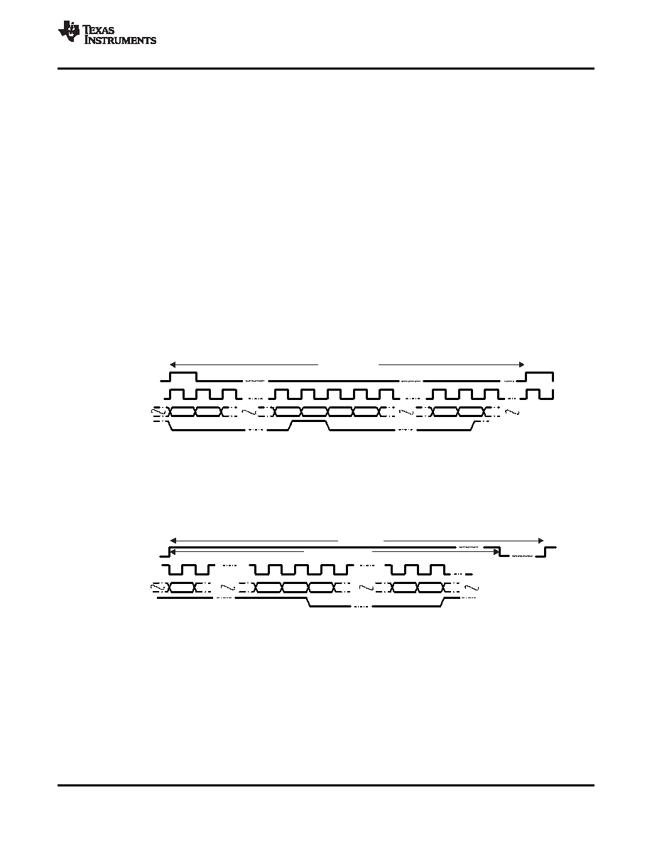
Figure 14. Both Channels Enabled, Early 3-Stating Enabled
Either or both of the two channels can be disabled in LJF, I2S, and DSP modes by using page 0 / register 38,
bits D3–D2. Figure 14 shows the interface timing when both channels are enabled and early 3-stating is enabled.
Figure 15 shows the effect of setting page 0 / register 38, bit D2, first channel disabled, and setting page 0 /
register 27, bit D0 to 1, which enables placing DOUT in the high-impedance state. If placing DOUT in the
high-impedance state is disabled, then the DOUT signal is driven to logic level 0.
Figure 15. First Channel Disabled, Second Channel Enabled, 3-Stating Enabled
The sync signal for the ADC filter is not generated based on the disabled channel. The sync signal for the filter
corresponds to the beginning of the earlier of the two channels. If the first channel is disabled, the filter sync is
generated at the beginning of the second channel, if it is enabled. If both the channels are disabled, there is no
output to the serial bus, and the filter sync corresponds to the beginning of the frame.
By default, when the word clocks and bit clocks are generated by the TLV320ADC3101, these clocks are active
only when the ADC is powered up within the device. This is done to save power. However, it also supports a
feature wherein both the word clocks and bit clocks can be active even when the codec in the device is powered
down. This is useful when using the TDM mode with multiple codecs on the same bus or when word clocks or bit
clocks are used in the system as general-purpose clocks.
Copyright 2008–2009, Texas Instruments Incorporated
17
Product Folder Link(s) :TLV320ADC3101
相关PDF资料 |
PDF描述 |
|---|---|
| TLV320ADC3101IRGET | SPECIALTY CONSUMER CIRCUIT, PQCC24 |
| TLV320AIC10C | SPECIALTY CONSUMER CIRCUIT, PQFP48 |
| TLV320AIC10I | SPECIALTY CONSUMER CIRCUIT, PQFP48 |
| TLV320AIC10CPFB | SPECIALTY CONSUMER CIRCUIT, PQFP48 |
| TLV320AIC10IPFB | SPECIALTY CONSUMER CIRCUIT, PQFP48 |
相关代理商/技术参数 |
参数描述 |
|---|---|
| TLV320ADC3101IRGET | 功能描述:音频模/数转换器 IC 92dB (16B) Low Power Stereo ADC RoHS:否 制造商:Wolfson Microelectronics 转换速率: 分辨率: ADC 输入端数量: 工作电源电压: 最大工作温度: 最小工作温度: 安装风格: 封装 / 箱体: 封装: |
| TLV320AIC10 | 制造商:TI 制造商全称:Texas Instruments 功能描述:General-Purpose 3V to 5.5V 16-bit 22-KSPS DSP CODEC |
| TLV320AIC10C | 制造商:TI 制造商全称:Texas Instruments 功能描述:General-Purpose 3V to 5.5V 16-bit 22-KSPS DSP CODEC |
| TLV320AIC10CGQER | 功能描述:接口—CODEC 16-Bit 22-KSPS DSP Codec RoHS:否 制造商:Texas Instruments 类型: 分辨率: 转换速率:48 kSPs 接口类型:I2C ADC 数量:2 DAC 数量:4 工作电源电压:1.8 V, 2.1 V, 2.3 V to 5.5 V 最大工作温度:+ 85 C 安装风格:SMD/SMT 封装 / 箱体:DSBGA-81 封装:Reel |
| TLV320AIC10CPFB | 功能描述:接口—CODEC 16-Bit 22-KSPS DSP Codec RoHS:否 制造商:Texas Instruments 类型: 分辨率: 转换速率:48 kSPs 接口类型:I2C ADC 数量:2 DAC 数量:4 工作电源电压:1.8 V, 2.1 V, 2.3 V to 5.5 V 最大工作温度:+ 85 C 安装风格:SMD/SMT 封装 / 箱体:DSBGA-81 封装:Reel |
发布紧急采购,3分钟左右您将得到回复。