- 您现在的位置:买卖IC网 > PDF目录98252 > TLV320ADC3101IRGER (TEXAS INSTRUMENTS INC) SPECIALTY CONSUMER CIRCUIT, PQCC24 PDF资料下载
参数资料
| 型号: | TLV320ADC3101IRGER |
| 厂商: | TEXAS INSTRUMENTS INC |
| 元件分类: | 消费家电 |
| 英文描述: | SPECIALTY CONSUMER CIRCUIT, PQCC24 |
| 封装: | GREEN, PLASTIC, VQFN-24 |
| 文件页数: | 46/84页 |
| 文件大小: | 1363K |
| 代理商: | TLV320ADC3101IRGER |
第1页第2页第3页第4页第5页第6页第7页第8页第9页第10页第11页第12页第13页第14页第15页第16页第17页第18页第19页第20页第21页第22页第23页第24页第25页第26页第27页第28页第29页第30页第31页第32页第33页第34页第35页第36页第37页第38页第39页第40页第41页第42页第43页第44页第45页当前第46页第47页第48页第49页第50页第51页第52页第53页第54页第55页第56页第57页第58页第59页第60页第61页第62页第63页第64页第65页第66页第67页第68页第69页第70页第71页第72页第73页第74页第75页第76页第77页第78页第79页第80页第81页第82页第83页第84页
SLAS553A – NOVEMBER 2008 – REVISED SEPTEMBER 2009...................................................................................................................................... www.ti.com
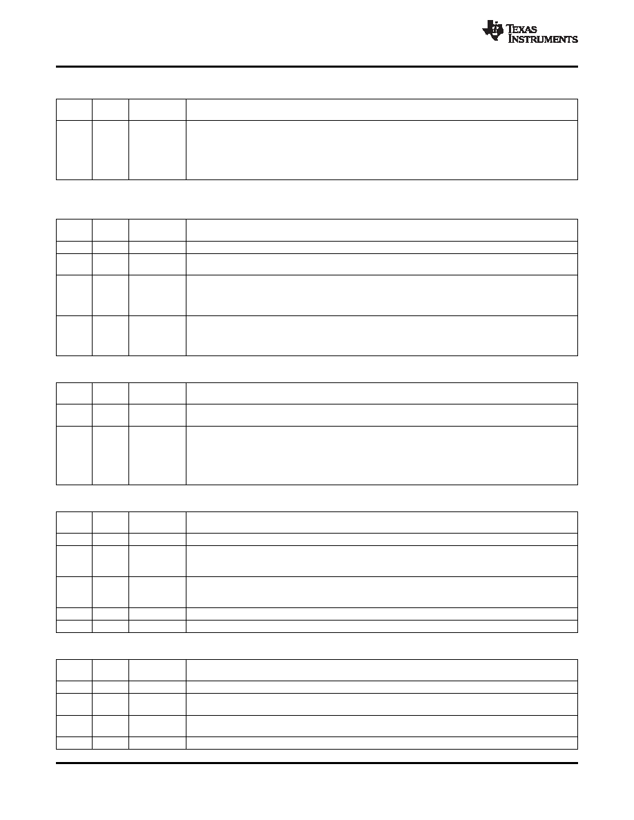
Page 0 / Register 28: Data Slot Offset Programmability 1 (Ch_Offset_1)
READ/
RESET
BIT
DESCRIPTION
WRITE
VALUE
D7–D0
R/W
0000 0000
0000 0000: Offset = 0 BCLKs. Offset is measured with respect to WCLK rising edge in DSP mode.(1)
0000 0001: Offset = 1 BCLKs
0000 0010: Offset = 2 BCLKs
...
1111 1110: Offset = 254 BCLKs
1111 1111: Offset = 255 BCLKs
(1)
Usage controlled by page 0 / register 38, bit D0
Page 0 / Register 29: ADC Interface Control 2
READ/
RESET
BIT
DESCRIPTION
WRITE
VALUE
D7–D4
R/W
0000
Reserved. Do not write any value other than reset value.
D3
R/W
0
0: BCLK is not inverted (valid for both primary and secondary BCLK).
1: BCLK is inverted (valid for both primary and secondary BCLK).
D2
R/W
0
0: BCLK and WCLK active even with codec powered down: disabled (valid for both primary and
secondary BCLK)
1: BCLK and WCLK active even with codec powered down: enabled (valid for both primary and
secondary BCLK)
D1–D0
R/W
10
00: Reserved. Do not use.
01: Reserved. Do not use.
10: BDIV_CLKIN = ADC_CLK (generated on-chip)
11: BDIV_CLKIN = ADC_MOD_CLK (generated on-chip)
Page 0 / Register 30: BCLK N Divider
READ/
RESET
BIT
DESCRIPTION
WRITE
VALUE
D7
R/W
0
0: BCLK N divider is powered down.
1: BCLK N divider is powered up.
D6–D0
R/W
000 0001
000 0000: CLKOUT divider N = 128
000 0001: CLKOUT divider N = 1
000 0010: CLKOUT divider N = 2
...
111 1110: CLKOUT divider N = 126
111 1111: CLKOUT divider N = 127
Page 0 / Register 31: Secondary Audio Interface Control 1
READ/
RESET
BIT
DESCRIPTION
WRITE
VALUE
D7
R
0
Reserved. Do not write any value other than reset value.
D6–D5
R/W
00
00: Secondary BCLK is obtained from GPIO1 pin.
01: Secondary BCLK is obtained from GPIO2 pin.
10 – 11: Reserved. Do not use.
D4–D3
R/W
00
00: Secondary WCLK is obtained from GPIO1 pin.
01: Secondary WCLK is obtained from GPIO2 pin.
10 – 11: Reserved. Do not use.
D2-D1
R/W
00
Reserved. Do not use.
D0
R
0
Reserved. Do not write any value other than reset value.
Page 0 / Register 32: Secondary Audio Interface Control 2
READ/
RESET
BIT
DESCRIPTION
WRITE
VALUE
D7–D4
R
0000
Reserved. Do not write any value other than reset value.
D3
R/W
0
0: Primary BCLK is used for audio interface and clocking.
1: Secondary BCLK is used for audio interface and clocking.
D2
R/W
0
0: Primary WCLK is used for audio interface and clocking.
1: Secondary WCLK is used for audio interface and clocking.
D1–D0
R
00
Reserved. Do not write any value other than reset value.
50
Copyright 2008–2009, Texas Instruments Incorporated
Product Folder Link(s) :TLV320ADC3101
相关PDF资料 |
PDF描述 |
|---|---|
| TLV320ADC3101IRGET | SPECIALTY CONSUMER CIRCUIT, PQCC24 |
| TLV320AIC10C | SPECIALTY CONSUMER CIRCUIT, PQFP48 |
| TLV320AIC10I | SPECIALTY CONSUMER CIRCUIT, PQFP48 |
| TLV320AIC10CPFB | SPECIALTY CONSUMER CIRCUIT, PQFP48 |
| TLV320AIC10IPFB | SPECIALTY CONSUMER CIRCUIT, PQFP48 |
相关代理商/技术参数 |
参数描述 |
|---|---|
| TLV320ADC3101IRGET | 功能描述:音频模/数转换器 IC 92dB (16B) Low Power Stereo ADC RoHS:否 制造商:Wolfson Microelectronics 转换速率: 分辨率: ADC 输入端数量: 工作电源电压: 最大工作温度: 最小工作温度: 安装风格: 封装 / 箱体: 封装: |
| TLV320AIC10 | 制造商:TI 制造商全称:Texas Instruments 功能描述:General-Purpose 3V to 5.5V 16-bit 22-KSPS DSP CODEC |
| TLV320AIC10C | 制造商:TI 制造商全称:Texas Instruments 功能描述:General-Purpose 3V to 5.5V 16-bit 22-KSPS DSP CODEC |
| TLV320AIC10CGQER | 功能描述:接口—CODEC 16-Bit 22-KSPS DSP Codec RoHS:否 制造商:Texas Instruments 类型: 分辨率: 转换速率:48 kSPs 接口类型:I2C ADC 数量:2 DAC 数量:4 工作电源电压:1.8 V, 2.1 V, 2.3 V to 5.5 V 最大工作温度:+ 85 C 安装风格:SMD/SMT 封装 / 箱体:DSBGA-81 封装:Reel |
| TLV320AIC10CPFB | 功能描述:接口—CODEC 16-Bit 22-KSPS DSP Codec RoHS:否 制造商:Texas Instruments 类型: 分辨率: 转换速率:48 kSPs 接口类型:I2C ADC 数量:2 DAC 数量:4 工作电源电压:1.8 V, 2.1 V, 2.3 V to 5.5 V 最大工作温度:+ 85 C 安装风格:SMD/SMT 封装 / 箱体:DSBGA-81 封装:Reel |
发布紧急采购,3分钟左右您将得到回复。