- 您现在的位置:买卖IC网 > PDF目录300033 > TMP86FS49AUG 8-BIT, FLASH, 16 MHz, MICROCONTROLLER, PQFP64 PDF资料下载
参数资料
| 型号: | TMP86FS49AUG |
| 元件分类: | 微控制器/微处理器 |
| 英文描述: | 8-BIT, FLASH, 16 MHz, MICROCONTROLLER, PQFP64 |
| 封装: | 10 X 10 MM, 0.50 MM PITCH, LEAD FREE, PLASTIC, LQFP-64 |
| 文件页数: | 97/277页 |
| 文件大小: | 2632K |
| 代理商: | TMP86FS49AUG |
第1页第2页第3页第4页第5页第6页第7页第8页第9页第10页第11页第12页第13页第14页第15页第16页第17页第18页第19页第20页第21页第22页第23页第24页第25页第26页第27页第28页第29页第30页第31页第32页第33页第34页第35页第36页第37页第38页第39页第40页第41页第42页第43页第44页第45页第46页第47页第48页第49页第50页第51页第52页第53页第54页第55页第56页第57页第58页第59页第60页第61页第62页第63页第64页第65页第66页第67页第68页第69页第70页第71页第72页第73页第74页第75页第76页第77页第78页第79页第80页第81页第82页第83页第84页第85页第86页第87页第88页第89页第90页第91页第92页第93页第94页第95页第96页当前第97页第98页第99页第100页第101页第102页第103页第104页第105页第106页第107页第108页第109页第110页第111页第112页第113页第114页第115页第116页第117页第118页第119页第120页第121页第122页第123页第124页第125页第126页第127页第128页第129页第130页第131页第132页第133页第134页第135页第136页第137页第138页第139页第140页第141页第142页第143页第144页第145页第146页第147页第148页第149页第150页第151页第152页第153页第154页第155页第156页第157页第158页第159页第160页第161页第162页第163页第164页第165页第166页第167页第168页第169页第170页第171页第172页第173页第174页第175页第176页第177页第178页第179页第180页第181页第182页第183页第184页第185页第186页第187页第188页第189页第190页第191页第192页第193页第194页第195页第196页第197页第198页第199页第200页第201页第202页第203页第204页第205页第206页第207页第208页第209页第210页第211页第212页第213页第214页第215页第216页第217页第218页第219页第220页第221页第222页第223页第224页第225页第226页第227页第228页第229页第230页第231页第232页第233页第234页第235页第236页第237页第238页第239页第240页第241页第242页第243页第244页第245页第246页第247页第248页第249页第250页第251页第252页第253页第254页第255页第256页第257页第258页第259页第260页第261页第262页第263页第264页第265页第266页第267页第268页第269页第270页第271页第272页第273页第274页第275页第276页第277页
186
ATmega165A/PA/325A/PA/3250A/PA/645A/P/6450A/P [DATASHEET]
8285E–AVR–02/2013
Note:
1. The DI and USCK pins are renamed to Serial Data (SDA) and Serial Clock (SCL) respectively to avoid confusion
between the modes of operation.
Bit 3:2 – USICS1:0: Clock Source Select
These bits set the clock source for the Shift Register and counter. The data output latch ensures that the output is
changed at the opposite edge of the sampling of the data input (DI/SDA) when using external clock source
(USCK/SCL). When software strobe or Timer/Counter0 Compare Match clock option is selected, the output latch is
transparent and therefore the output is changed immediately. Clearing the USICS1...0 bits enables software strobe
option. When using this option, writing a one to the USICLK bit clocks both the Shift Register and the counter. For
external clock source (USICS1 = 1), the USICLK bit is no longer used as a strobe, but selects between external
clocking and software clocking by the USITC strobe bit.
Table 21-2 shows the relationship between the USICS1:0 and USICLK setting and clock source used for the Shift
Register and the 4-bit counter.
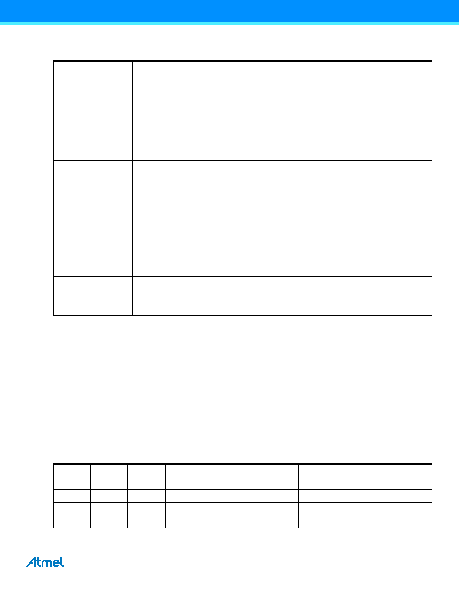
Table 21-1.
Relations between USIWM1:0 and the USI Operation
USIWM1
USIWM0
Description
0
Outputs, clock hold, and start detector disabled. Port pins operates as normal.
01
Three-wire mode. Uses DO, DI, and USCK pins.
The Data Output (DO) pin overrides the corresponding bit in the PORT Register in this mode.
However, the corresponding DDR bit still controls the data direction. When the port pin is set as
input the pins pull-up is controlled by the PORT bit.
The Data Input (DI) and Serial Clock (USCK) pins do not affect the normal port operation. When
operating as master, clock pulses are software generated by toggling the PORT Register, while
the data direction is set to output. The USITC bit in the USICR Register can be used for this
purpose.
10
Two-wire mode. Uses SDA (DI) and SCL (USCK) pins (1).
The Serial Data (SDA) and the Serial Clock (SCL) pins are bi-directional and uses open-collector
output drives. The output drivers are enabled by setting the corresponding bit for SDA and SCL in
the DDR Register.
When the output driver is enabled for the SDA pin, the output driver will force the line SDA low if
the output of the Shift Register or the corresponding bit in the PORT Register is zero. Otherwise
the SDA line will not be driven (i.e., it is released). When the SCL pin output driver is enabled the
SCL line will be forced low if the corresponding bit in the PORT Register is zero, or by the start
detector. Otherwise the SCL line will not be driven.
The SCL line is held low when a start detector detects a start condition and the output is enabled.
Clearing the Start Condition Flag (USISIF) releases the line. The SDA and SCL pin inputs is not
affected by enabling this mode. Pull-ups on the SDA and SCL port pin are disabled in Two-wire
mode.
11
Two-wire mode. Uses SDA and SCL pins.
Same operation as for the Two-wire mode described above, except that the SCL line is also held
low when a counter overflow occurs, and is held low until the Counter Overflow Flag (USIOIF) is
cleared.
Table 21-2.
Relations between the USICS1:0 and USICLK setting.
USICS1
USICS0
USICLK
Shift Register Clock Source
4-bit Counter Clock Source
0
No Clock
0
1
Software clock strobe (USICLK)
0
1
X
Timer/Counter0 Compare Match
1
0
External, positive edge
External, both edges
相关PDF资料 |
PDF描述 |
|---|---|
| TMP86FS64FG | 8-BIT, FLASH, 16 MHz, MICROCONTROLLER, PQFP100 |
| TMP87P409N | 8-BIT, MROM, 8 MHz, MICROCONTROLLER, PDIP28 |
| TMP87P808NG | 8-BIT, OTPROM, 8 MHz, MICROCONTROLLER, PDIP28 |
| TMP87PM14FG | 8-BIT, OTPROM, 8 MHz, MICROCONTROLLER, PQFP64 |
| TMP88CM38AFG | 8-BIT, MROM, 24 MHz, MICROCONTROLLER, PQFP44 |
相关代理商/技术参数 |
参数描述 |
|---|---|
| TMP86FS49AUG(JZ) | 功能描述:8位微控制器 -MCU 60K Flash MCU RoHS:否 制造商:Silicon Labs 核心:8051 处理器系列:C8051F39x 数据总线宽度:8 bit 最大时钟频率:50 MHz 程序存储器大小:16 KB 数据 RAM 大小:1 KB 片上 ADC:Yes 工作电源电压:1.8 V to 3.6 V 工作温度范围:- 40 C to + 105 C 封装 / 箱体:QFN-20 安装风格:SMD/SMT |
| TMP86FS49AUG(Z) | 制造商:Toshiba America Electronic Components 功能描述:MCU 8BIT TLCS-870 CISC 60KB FLASH 5V 64LQFP - Bulk |
| TMP86FS49BFG | 制造商:TOSHIBA 制造商全称:Toshiba Semiconductor 功能描述:8 Bit Microcontroller |
| TMP86FS49BFG(CZHZ) | 制造商:Toshiba America Electronic Components 功能描述:INTEGRATED CIRCUIT MICROCONTROLLER TLCS870C- CU WIRE - Bulk |
| TMP86FS49BFG(ZHZ) | 功能描述:8位微控制器 -MCU INTEGRATED CIRCUIT MICROCONTROLLER TLCS870C RoHS:否 制造商:Silicon Labs 核心:8051 处理器系列:C8051F39x 数据总线宽度:8 bit 最大时钟频率:50 MHz 程序存储器大小:16 KB 数据 RAM 大小:1 KB 片上 ADC:Yes 工作电源电压:1.8 V to 3.6 V 工作温度范围:- 40 C to + 105 C 封装 / 箱体:QFN-20 安装风格:SMD/SMT |
发布紧急采购,3分钟左右您将得到回复。