- 您现在的位置:买卖IC网 > PDF目录382635 > TMS320F243PGEQ 16-Bit Digital Signal Processor PDF资料下载
参数资料
| 型号: | TMS320F243PGEQ |
| 元件分类: | 数字信号处理 |
| 英文描述: | 16-Bit Digital Signal Processor |
| 中文描述: | 16位数字信号处理器 |
| 文件页数: | 15/116页 |
| 文件大小: | 1485K |
| 代理商: | TMS320F243PGEQ |
第1页第2页第3页第4页第5页第6页第7页第8页第9页第10页第11页第12页第13页第14页当前第15页第16页第17页第18页第19页第20页第21页第22页第23页第24页第25页第26页第27页第28页第29页第30页第31页第32页第33页第34页第35页第36页第37页第38页第39页第40页第41页第42页第43页第44页第45页第46页第47页第48页第49页第50页第51页第52页第53页第54页第55页第56页第57页第58页第59页第60页第61页第62页第63页第64页第65页第66页第67页第68页第69页第70页第71页第72页第73页第74页第75页第76页第77页第78页第79页第80页第81页第82页第83页第84页第85页第86页第87页第88页第89页第90页第91页第92页第93页第94页第95页第96页第97页第98页第99页第100页第101页第102页第103页第104页第105页第106页第107页第108页第109页第110页第111页第112页第113页第114页第115页第116页
TMS320F243, TMS320F241
DSP CONTROLLERS
SPRS064B – DECEMBER 1997 – REVISED FEBRUARY 1999
15
POST OFFICE BOX 1443
HOUSTON, TEXAS 77251–1443
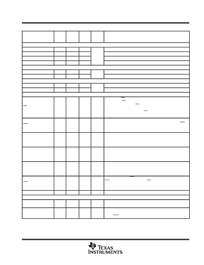
Terminal Functions - ’F241 PG and FN Packages (Continued)
NAME
64
QFP
NO.
68
PLCC
NO.
TYPE
RESET
STATE
DESCRIPTION
SERIAL PERIPHERAL INTERFACE (SPI) AND BIT I/O PINS
56
I/O
SPI slave in, master out or GPIO
SPISIMO/
IOPC2
SPISOMI/
IOPC3
SPICLK/
IOPC4
SPISTE/
IOPC5
45
46
57
I/O
I
SPI slave out, master in or GPIO
47
58
I/O
SPI clock or GPIO
48
59
I/O
SPI slave transmit enable (optional) or GPIO
SERIAL COMMUNICATIONS INTERFACE (SCI) AND BIT I/O PINS
54
I/O
55
I/O
SCI asynchronous serial port receive data or GPIO
SCITXD/
IOPA0
SCIRXD/
IOPA1
43
SCI asynchronous serial port transmit data or GPIO
44
I
CONTROLLER AREA NETWORK (CAN)
I/O
I/O
CAN receive data or GPIO
CANTX/
IOPC6
CANRX/
IOPC7
4
11
CAN transmit data or GPIO
3
10
I
INTERRUPT, EXTERNAL ACCESS, AND MISCELLANEOUS SIGNALS
RS
27
35
I/O
I
Device reset. RS causes the ’F243/241 to terminate execution and sets
PC = 0. When RS is brought to a high level, execution begins at location
zero of program memory. RS affects (or sets to zero) various registers
and status bits. When the watchdog timer overflows, it initiates a system
reset pulse that is reflected on the RS pin. This pulse is eight clock cycles
wide.
NMI§
53
64
I
I
Nonmaskable interrupt. When NMI is activated, the device is interrupted
regardless of the state of the INTM bit of the status register. NMI is
(falling) edge- and low-level-sensitive. To be recognized by the core, this
pin must be kept low for at least one clock cycle after the falling edge.
XINT1/
IOPA2
55
66
I/O
I
External user interrupt 1 or GPIO. Both XINT1 and XINT2 are edge-
sensitive. To be recognized by the core, these pins must be kept low/high
for at least one clock cycle after the edge. The edge polarity is
programmable.
XINT2/ADCSOC/
IOPD1
54
65
I/O
I
External user interrupt 2. External “start-of-conversion” input for
ADC/GPIO. Both XINT1 and XINT2 are edge-sensitive. To be
recognized by the core, these pins must be kept low/high for at least one
clock cycle after the edge. The edge polarity is programmable.
XF
/IOPC0
39
50
I/O
O – 1
External flag output (latched software-programmable signal). XF is a
general-purpose output pin. It is set/reset by the
SETC XF/CLRC XF
instruction. This pin is configured as an external flag output by all device
resets. It can be used as a GPIO, if not used as XF.
BIO
/IOPC1
42
53
I/O
I
Branch control input. BIO is polled by the
BCND pma,BIO
instruction. If
BIO is low, a branch is executed. If BIO is not used, it should be pulled
high. This pin is configured as a branch control input by all device resets.
It can be used as a GPIO, if not used as a branch control input.
PMT
49
60
I
I
Enables parallel module test (PMT). Do not connect, reserved for test.
CLOCK SIGNALS
XTAL1/CLKIN
35
46
I
I
PLL oscillator input pin. Crystal input to PLL/clock source input to PLL.
XTAL1/CLKIN is tied to one side of a reference crystal.
XTAL2
36
47
O
O
Crystal output. PLL oscillator output pin. XTAL2 is tied to one side of a
reference crystal. This pin goes in the high-impedance state when
EMU1/OFF is active low.
I = input, O = output, Z = high impedance
The reset state indicates the state of the pin at reset. If the pin is an input, indicated by an I, its state is determined by user design. If the pin is
an output, its level at reset is indicated.
§ In silicon revisions 2.0-TMX and 2.1-TMS, this pin is level-sensitive and can cause multiple interrupts when held low.
NOTE:
Bold, italicized pin names
indicate pin function after reset.
相关PDF资料 |
PDF描述 |
|---|---|
| TMS320F243PGES | 16-Bit Digital Signal Processor |
| TMS320C3X | 32-Bit Digital Signal Processor |
| TMS320C4X | Digital Signal Processing Solutions |
| TMS320C6454GTZ7 | Fixed-Point Digital Signal Processor |
| TMS320C6454GTZ | Fixed-Point Digital Signal Processor |
相关代理商/技术参数 |
参数描述 |
|---|---|
| TMS320F28015PZA | 功能描述:数字信号处理器和控制器 - DSP, DSC 32-Bit DSC w/ 32KB Flash RoHS:否 制造商:Microchip Technology 核心:dsPIC 数据总线宽度:16 bit 程序存储器大小:16 KB 数据 RAM 大小:2 KB 最大时钟频率:40 MHz 可编程输入/输出端数量:35 定时器数量:3 设备每秒兆指令数:50 MIPs 工作电源电压:3.3 V 最大工作温度:+ 85 C 封装 / 箱体:TQFP-44 安装风格:SMD/SMT |
| TMS320F28015PZA | 制造商:Texas Instruments 功能描述:IC DSP 32-BIT CMOS QFP 100PIN PLAS |
| TMS320F28015PZQ | 功能描述:数字信号处理器和控制器 - DSP, DSC 32-Bit DSC w/ 32KB Flash RoHS:否 制造商:Microchip Technology 核心:dsPIC 数据总线宽度:16 bit 程序存储器大小:16 KB 数据 RAM 大小:2 KB 最大时钟频率:40 MHz 可编程输入/输出端数量:35 定时器数量:3 设备每秒兆指令数:50 MIPs 工作电源电压:3.3 V 最大工作温度:+ 85 C 封装 / 箱体:TQFP-44 安装风格:SMD/SMT |
| TMS320F28015PZS | 功能描述:数字信号处理器和控制器 - DSP, DSC 32-Bit DSC w/ 32KB Flash RoHS:否 制造商:Microchip Technology 核心:dsPIC 数据总线宽度:16 bit 程序存储器大小:16 KB 数据 RAM 大小:2 KB 最大时钟频率:40 MHz 可编程输入/输出端数量:35 定时器数量:3 设备每秒兆指令数:50 MIPs 工作电源电压:3.3 V 最大工作温度:+ 85 C 封装 / 箱体:TQFP-44 安装风格:SMD/SMT |
| TMS320F28015ZGMA | 功能描述:数字信号处理器和控制器 - DSP, DSC 32B Dig Sig Cntrlr RoHS:否 制造商:Microchip Technology 核心:dsPIC 数据总线宽度:16 bit 程序存储器大小:16 KB 数据 RAM 大小:2 KB 最大时钟频率:40 MHz 可编程输入/输出端数量:35 定时器数量:3 设备每秒兆指令数:50 MIPs 工作电源电压:3.3 V 最大工作温度:+ 85 C 封装 / 箱体:TQFP-44 安装风格:SMD/SMT |
发布紧急采购,3分钟左右您将得到回复。