- 您现在的位置:买卖IC网 > PDF目录11226 > TMS320F28069UPZT (Texas Instruments)IC MCU 32BIT 256KB FLASH 100LQFP PDF资料下载
参数资料
| 型号: | TMS320F28069UPZT |
| 厂商: | Texas Instruments |
| 文件页数: | 139/174页 |
| 文件大小: | 0K |
| 描述: | IC MCU 32BIT 256KB FLASH 100LQFP |
| 产品培训模块: | ControlSUITE Piccolo F2806x TPS75005 Single IC Power for C2000 MCU |
| 标准包装: | 90 |
| 系列: | TMS320F2806x, Piccolo™, C2000™ |
| 核心处理器: | C28x |
| 芯体尺寸: | 32-位 |
| 速度: | 80MHz |
| 连通性: | CAN,I²C,McBSP,SCI,SPI,UART/USART |
| 外围设备: | 欠压检测/复位,DMA,POR,PWM,WDT |
| 输入/输出数: | 54 |
| 程序存储器容量: | 256KB(128K x 16) |
| 程序存储器类型: | 闪存 |
| RAM 容量: | 50K x 16 |
| 电压 - 电源 (Vcc/Vdd): | 1.71 V ~ 1.995 V |
| 数据转换器: | A/D 16x12b |
| 振荡器型: | 内部 |
| 工作温度: | -40°C ~ 105°C |
| 封装/外壳: | 100-LQFP |
| 包装: | 托盘 |
第1页第2页第3页第4页第5页第6页第7页第8页第9页第10页第11页第12页第13页第14页第15页第16页第17页第18页第19页第20页第21页第22页第23页第24页第25页第26页第27页第28页第29页第30页第31页第32页第33页第34页第35页第36页第37页第38页第39页第40页第41页第42页第43页第44页第45页第46页第47页第48页第49页第50页第51页第52页第53页第54页第55页第56页第57页第58页第59页第60页第61页第62页第63页第64页第65页第66页第67页第68页第69页第70页第71页第72页第73页第74页第75页第76页第77页第78页第79页第80页第81页第82页第83页第84页第85页第86页第87页第88页第89页第90页第91页第92页第93页第94页第95页第96页第97页第98页第99页第100页第101页第102页第103页第104页第105页第106页第107页第108页第109页第110页第111页第112页第113页第114页第115页第116页第117页第118页第119页第120页第121页第122页第123页第124页第125页第126页第127页第128页第129页第130页第131页第132页第133页第134页第135页第136页第137页第138页当前第139页第140页第141页第142页第143页第144页第145页第146页第147页第148页第149页第150页第151页第152页第153页第154页第155页第156页第157页第158页第159页第160页第161页第162页第163页第164页第165页第166页第167页第168页第169页第170页第171页第172页第173页第174页
th(boot-mode)(A)
tw(RSL2)
INTOSC1
X1/X2
XRS
Boot-Mode
Pins
XCLKOUT
I/O Pins
Address/Data/
Control
(Internal)
Boot-ROM Execution Starts
User-Code Execution Starts
User-Code Dependent
User-Code Execution Phase
User-Code Dependent
User-Code Execution
Peripheral/GPIO Function
User-Code Dependent
GPIO Pins as Input (State Depends on Internal PU/PD)
GPIO Pins as Input
Peripheral/GPIO Function
td(EX)
SPRS698D – NOVEMBER 2010 – REVISED DECEMBER 2012
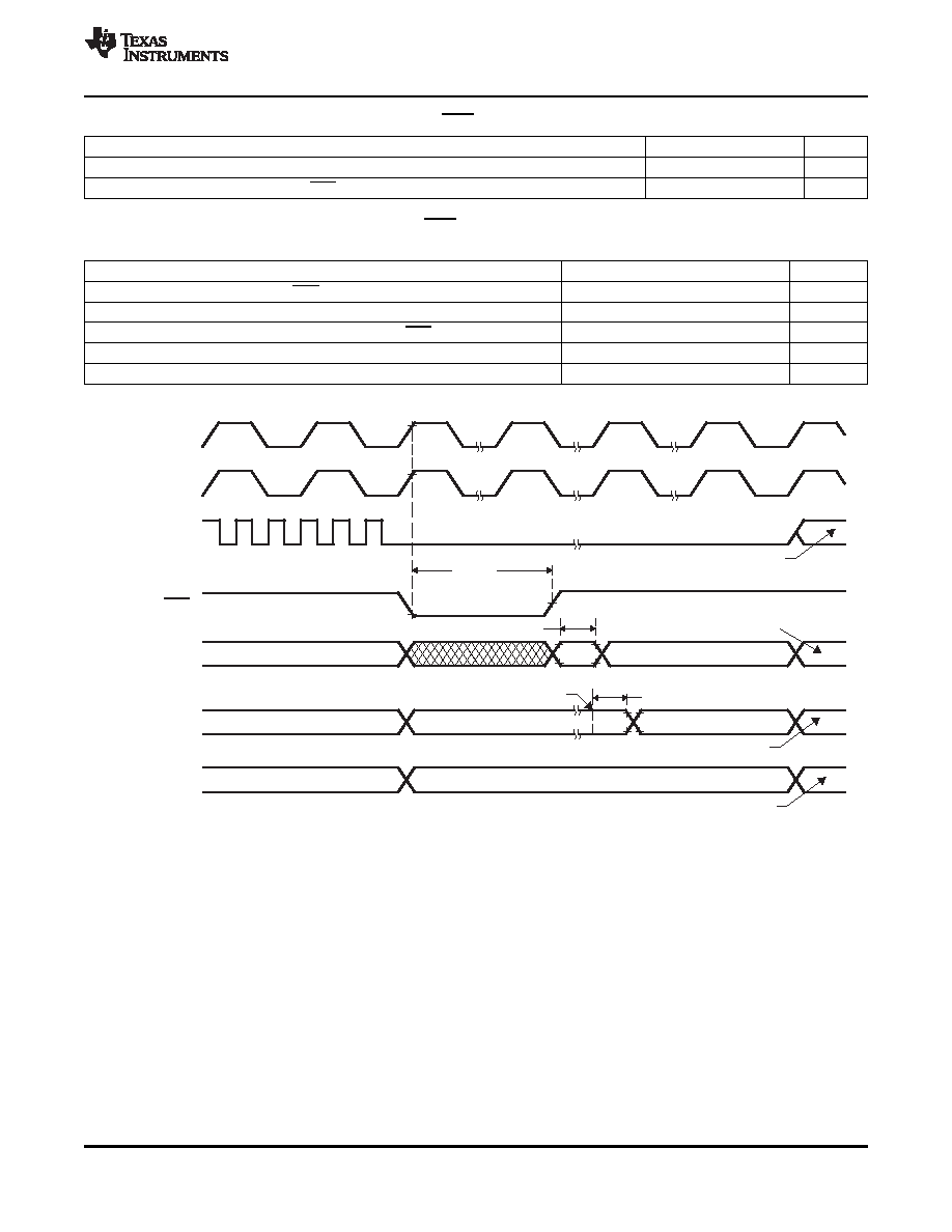
Table 5-7. Reset (XRS) Timing Requirements
MIN
MAX
UNIT
th(boot-mode)
Hold time for boot-mode pins
1000tc(SCO)
cycles
tw(RSL2)
Pulse duration, XRS low on warm reset
32tc(OSCCLK)
cycles
Table 5-8. Reset (XRS) Switching Characteristics
over recommended operating conditions (unless otherwise noted)
PARAMETER
MIN
TYP
MAX
UNIT
tw(RSL1)
Pulse duration, XRS driven by device
600
μs
tw(WDRS)
Pulse duration, reset pulse generated by watchdog
512tc(OSCCLK)
cycles
td(EX)
Delay time, address/data valid after XRS high
32tc(OSCCLK)
cycles
tINTOSCST
Start up time, internal zero-pin oscillator
3
μs
tOSCST
(1)
On-chip crystal-oscillator start-up time
1
10
ms
(1)
Dependent on crystal/resonator and board design.
A.
After reset, the Boot ROM code samples BOOT Mode pins. Based on the status of the Boot Mode pin, the boot code
branches to destination memory or boot code function. If Boot ROM code executes after power-on conditions (in
debugger environment), the Boot code execution time is based on the current SYSCLKOUT speed. The
SYSCLKOUT will be based on user environment and could be with or without PLL enabled.
Figure 5-5. Warm Reset
Copyright 2010–2012, Texas Instruments Incorporated
Peripheral and Electrical Specifications
67
相关PDF资料 |
PDF描述 |
|---|---|
| ADG408BR-REEL | IC MULTIPLEXER 8X1 16SOIC |
| ADV3221ARZ-R7 | IC MULTIPLEXER 4:1 16SOIC |
| ADG409BR-REEL | IC MULTIPLEXER DUAL 4X1 16SOIC |
| ADG408BRU-REEL | IC MULTIPLEXER 8X1 16TSSOP |
| DSPIC30F6013T-30I/PF | IC DSPIC MCU/DSP 132K 80TQFP |
相关代理商/技术参数 |
参数描述 |
|---|---|
| TMS320F2806GGMA | 功能描述:数字信号处理器和控制器 - DSP, DSC 32-Bit Digital Sig Controller w/Flash RoHS:否 制造商:Microchip Technology 核心:dsPIC 数据总线宽度:16 bit 程序存储器大小:16 KB 数据 RAM 大小:2 KB 最大时钟频率:40 MHz 可编程输入/输出端数量:35 定时器数量:3 设备每秒兆指令数:50 MIPs 工作电源电压:3.3 V 最大工作温度:+ 85 C 封装 / 箱体:TQFP-44 安装风格:SMD/SMT |
| TMS320F2806GGMS | 功能描述:数字信号处理器和控制器 - DSP, DSC 32-Bit Digital Sig Controller w/Flash RoHS:否 制造商:Microchip Technology 核心:dsPIC 数据总线宽度:16 bit 程序存储器大小:16 KB 数据 RAM 大小:2 KB 最大时钟频率:40 MHz 可编程输入/输出端数量:35 定时器数量:3 设备每秒兆指令数:50 MIPs 工作电源电压:3.3 V 最大工作温度:+ 85 C 封装 / 箱体:TQFP-44 安装风格:SMD/SMT |
| TMS320F2806PZA | 功能描述:数字信号处理器和控制器 - DSP, DSC 32-Bit Digital Sig Controller w/Flash RoHS:否 制造商:Microchip Technology 核心:dsPIC 数据总线宽度:16 bit 程序存储器大小:16 KB 数据 RAM 大小:2 KB 最大时钟频率:40 MHz 可编程输入/输出端数量:35 定时器数量:3 设备每秒兆指令数:50 MIPs 工作电源电压:3.3 V 最大工作温度:+ 85 C 封装 / 箱体:TQFP-44 安装风格:SMD/SMT |
| TMS320F2806PZQ | 功能描述:数字信号处理器和控制器 - DSP, DSC 32B Dig Signal Controller RoHS:否 制造商:Microchip Technology 核心:dsPIC 数据总线宽度:16 bit 程序存储器大小:16 KB 数据 RAM 大小:2 KB 最大时钟频率:40 MHz 可编程输入/输出端数量:35 定时器数量:3 设备每秒兆指令数:50 MIPs 工作电源电压:3.3 V 最大工作温度:+ 85 C 封装 / 箱体:TQFP-44 安装风格:SMD/SMT |
| TMS320F2806PZS | 功能描述:数字信号处理器和控制器 - DSP, DSC 32-Bit Digital Sig Controller w/Flash RoHS:否 制造商:Microchip Technology 核心:dsPIC 数据总线宽度:16 bit 程序存储器大小:16 KB 数据 RAM 大小:2 KB 最大时钟频率:40 MHz 可编程输入/输出端数量:35 定时器数量:3 设备每秒兆指令数:50 MIPs 工作电源电压:3.3 V 最大工作温度:+ 85 C 封装 / 箱体:TQFP-44 安装风格:SMD/SMT |
发布紧急采购,3分钟左右您将得到回复。