- 您现在的位置:买卖IC网 > PDF目录11226 > TMS320F28069UPZT (Texas Instruments)IC MCU 32BIT 256KB FLASH 100LQFP PDF资料下载
参数资料
| 型号: | TMS320F28069UPZT |
| 厂商: | Texas Instruments |
| 文件页数: | 89/174页 |
| 文件大小: | 0K |
| 描述: | IC MCU 32BIT 256KB FLASH 100LQFP |
| 产品培训模块: | ControlSUITE Piccolo F2806x TPS75005 Single IC Power for C2000 MCU |
| 标准包装: | 90 |
| 系列: | TMS320F2806x, Piccolo™, C2000™ |
| 核心处理器: | C28x |
| 芯体尺寸: | 32-位 |
| 速度: | 80MHz |
| 连通性: | CAN,I²C,McBSP,SCI,SPI,UART/USART |
| 外围设备: | 欠压检测/复位,DMA,POR,PWM,WDT |
| 输入/输出数: | 54 |
| 程序存储器容量: | 256KB(128K x 16) |
| 程序存储器类型: | 闪存 |
| RAM 容量: | 50K x 16 |
| 电压 - 电源 (Vcc/Vdd): | 1.71 V ~ 1.995 V |
| 数据转换器: | A/D 16x12b |
| 振荡器型: | 内部 |
| 工作温度: | -40°C ~ 105°C |
| 封装/外壳: | 100-LQFP |
| 包装: | 托盘 |
第1页第2页第3页第4页第5页第6页第7页第8页第9页第10页第11页第12页第13页第14页第15页第16页第17页第18页第19页第20页第21页第22页第23页第24页第25页第26页第27页第28页第29页第30页第31页第32页第33页第34页第35页第36页第37页第38页第39页第40页第41页第42页第43页第44页第45页第46页第47页第48页第49页第50页第51页第52页第53页第54页第55页第56页第57页第58页第59页第60页第61页第62页第63页第64页第65页第66页第67页第68页第69页第70页第71页第72页第73页第74页第75页第76页第77页第78页第79页第80页第81页第82页第83页第84页第85页第86页第87页第88页当前第89页第90页第91页第92页第93页第94页第95页第96页第97页第98页第99页第100页第101页第102页第103页第104页第105页第106页第107页第108页第109页第110页第111页第112页第113页第114页第115页第116页第117页第118页第119页第120页第121页第122页第123页第124页第125页第126页第127页第128页第129页第130页第131页第132页第133页第134页第135页第136页第137页第138页第139页第140页第141页第142页第143页第144页第145页第146页第147页第148页第149页第150页第151页第152页第153页第154页第155页第156页第157页第158页第159页第160页第161页第162页第163页第164页第165页第166页第167页第168页第169页第170页第171页第172页第173页第174页
SPRS698D – NOVEMBER 2010 – REVISED DECEMBER 2012
2.4
Signal Descriptions
Table 2-5 describes the signals. With the exception of the JTAG pins, the GPIO function is the default at
reset, unless otherwise mentioned. The peripheral signals that are listed under them are alternate
functions. Some peripheral functions may not be available in all devices. See Table 2-1 for details. Inputs
are not 5-V tolerant. All GPIO pins are I/O/Z and have an internal pullup, which can be selectively enabled
or disabled on a per-pin basis. This feature only applies to the GPIO pins. The pullups on the PWM pins
are not enabled at reset. The pullups on other GPIO pins are enabled upon reset. The AIO pins do not
have an internal pullup.
NOTE: When the on-chip VREG is used, the GPIO19, GPIO34, GPIO35, GPIO36, GPIO37, and GPIO38
pins could glitch during power up. If this is unacceptable in an application, 1.8 V could be supplied
externally. There is no power-sequencing requirement when using an external 1.8-V supply. However, if
the 3.3-V transistors in the level-shifting output buffers of the I/O pins are powered prior to the 1.9-V
transistors, it is possible for the output buffers to turn on, causing a glitch to occur on the pin during power
up. To avoid this behavior, power the VDD pins prior to or simultaneously with the VDDIO pins, ensuring that
the VDD pins have reached 0.7 V before the VDDIO pins reach 0.7 V.
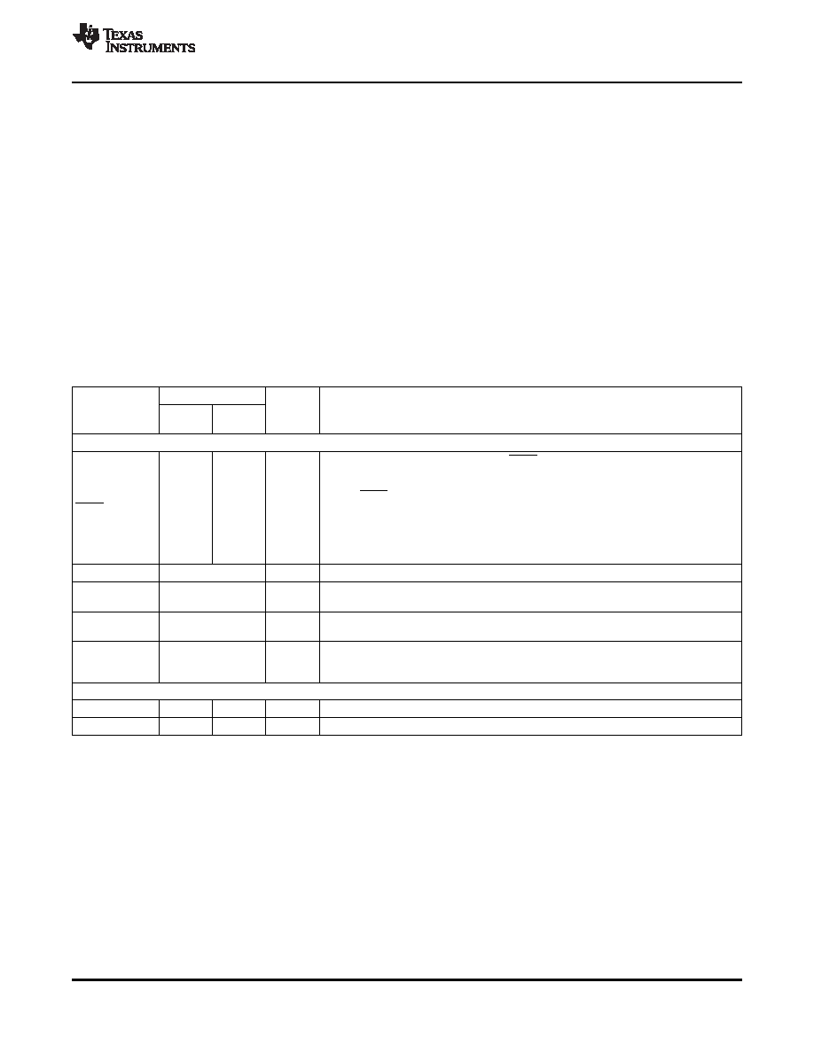
Table 2-5. Terminal Functions(1)
PIN NO.
PIN NAME
I/O/Z
DESCRIPTION
PZ
PN
PZP
PFP
JTAG
JTAG test reset with internal pulldown. TRST, when driven high, gives the scan system
control of the operations of the device. If this signal is not connected or driven low, the
device operates in its functional mode, and the test reset signals are ignored.
NOTE: TRST is an active-high test pin and must be maintained low at all times during
TRST
12
10
I
normal device operation. An external pull-down resistor is required on this pin. The
value of this resistor should be based on drive strength of the debugger pods
applicable to the design. A 2.2-k
resistor generally offers adequate protection. Since
this is application-specific, it is recommended that each target board be validated for
proper operation of the debugger and the application. (
↓)
TCK
See GPIO38
I
See GPIO38. JTAG test clock with internal pullup. (
↑)
See GPIO36. JTAG test-mode select (TMS) with internal pullup. This serial control
TMS
See GPIO36
I
input is clocked into the TAP controller on the rising edge of TCK. (
↑)
See GPIO35. JTAG test data input (TDI) with internal pullup. TDI is clocked into the
TDI
See GPIO35
I
selected register (instruction or data) on a rising edge of TCK. (
↑)
See GPIO37. JTAG scan out, test data output (TDO). The contents of the selected
TDO
See GPIO37
O/Z
register (instruction or data) are shifted out of TDO on the falling edge of TCK.
(8-mA drive)
FLASH
VDD3VFL
46
37
3.3-V Flash Core Power Pin. This pin should be connected to 3.3 V at all times.
TEST2
45
36
I/O
Test Pin. Reserved for TI. Must be left unconnected.
(1)
I = Input, O = Output, Z = High Impedance, OD = Open Drain,
↑ = Pullup, ↓ = Pulldown
Copyright 2010–2012, Texas Instruments Incorporated
Device Overview
21
相关PDF资料 |
PDF描述 |
|---|---|
| ADG408BR-REEL | IC MULTIPLEXER 8X1 16SOIC |
| ADV3221ARZ-R7 | IC MULTIPLEXER 4:1 16SOIC |
| ADG409BR-REEL | IC MULTIPLEXER DUAL 4X1 16SOIC |
| ADG408BRU-REEL | IC MULTIPLEXER 8X1 16TSSOP |
| DSPIC30F6013T-30I/PF | IC DSPIC MCU/DSP 132K 80TQFP |
相关代理商/技术参数 |
参数描述 |
|---|---|
| TMS320F2806GGMA | 功能描述:数字信号处理器和控制器 - DSP, DSC 32-Bit Digital Sig Controller w/Flash RoHS:否 制造商:Microchip Technology 核心:dsPIC 数据总线宽度:16 bit 程序存储器大小:16 KB 数据 RAM 大小:2 KB 最大时钟频率:40 MHz 可编程输入/输出端数量:35 定时器数量:3 设备每秒兆指令数:50 MIPs 工作电源电压:3.3 V 最大工作温度:+ 85 C 封装 / 箱体:TQFP-44 安装风格:SMD/SMT |
| TMS320F2806GGMS | 功能描述:数字信号处理器和控制器 - DSP, DSC 32-Bit Digital Sig Controller w/Flash RoHS:否 制造商:Microchip Technology 核心:dsPIC 数据总线宽度:16 bit 程序存储器大小:16 KB 数据 RAM 大小:2 KB 最大时钟频率:40 MHz 可编程输入/输出端数量:35 定时器数量:3 设备每秒兆指令数:50 MIPs 工作电源电压:3.3 V 最大工作温度:+ 85 C 封装 / 箱体:TQFP-44 安装风格:SMD/SMT |
| TMS320F2806PZA | 功能描述:数字信号处理器和控制器 - DSP, DSC 32-Bit Digital Sig Controller w/Flash RoHS:否 制造商:Microchip Technology 核心:dsPIC 数据总线宽度:16 bit 程序存储器大小:16 KB 数据 RAM 大小:2 KB 最大时钟频率:40 MHz 可编程输入/输出端数量:35 定时器数量:3 设备每秒兆指令数:50 MIPs 工作电源电压:3.3 V 最大工作温度:+ 85 C 封装 / 箱体:TQFP-44 安装风格:SMD/SMT |
| TMS320F2806PZQ | 功能描述:数字信号处理器和控制器 - DSP, DSC 32B Dig Signal Controller RoHS:否 制造商:Microchip Technology 核心:dsPIC 数据总线宽度:16 bit 程序存储器大小:16 KB 数据 RAM 大小:2 KB 最大时钟频率:40 MHz 可编程输入/输出端数量:35 定时器数量:3 设备每秒兆指令数:50 MIPs 工作电源电压:3.3 V 最大工作温度:+ 85 C 封装 / 箱体:TQFP-44 安装风格:SMD/SMT |
| TMS320F2806PZS | 功能描述:数字信号处理器和控制器 - DSP, DSC 32-Bit Digital Sig Controller w/Flash RoHS:否 制造商:Microchip Technology 核心:dsPIC 数据总线宽度:16 bit 程序存储器大小:16 KB 数据 RAM 大小:2 KB 最大时钟频率:40 MHz 可编程输入/输出端数量:35 定时器数量:3 设备每秒兆指令数:50 MIPs 工作电源电压:3.3 V 最大工作温度:+ 85 C 封装 / 箱体:TQFP-44 安装风格:SMD/SMT |
发布紧急采购,3分钟左右您将得到回复。