- 您现在的位置:买卖IC网 > PDF目录382626 > TMX320F2812GHHS (Texas Instruments, Inc.) DIGITAL SIGNAL PROCESSORS PDF资料下载
参数资料
| 型号: | TMX320F2812GHHS |
| 厂商: | Texas Instruments, Inc. |
| 元件分类: | 数字信号处理 |
| 英文描述: | DIGITAL SIGNAL PROCESSORS |
| 中文描述: | 数字信号处理器 |
| 文件页数: | 69/147页 |
| 文件大小: | 2021K |
| 代理商: | TMX320F2812GHHS |
第1页第2页第3页第4页第5页第6页第7页第8页第9页第10页第11页第12页第13页第14页第15页第16页第17页第18页第19页第20页第21页第22页第23页第24页第25页第26页第27页第28页第29页第30页第31页第32页第33页第34页第35页第36页第37页第38页第39页第40页第41页第42页第43页第44页第45页第46页第47页第48页第49页第50页第51页第52页第53页第54页第55页第56页第57页第58页第59页第60页第61页第62页第63页第64页第65页第66页第67页第68页当前第69页第70页第71页第72页第73页第74页第75页第76页第77页第78页第79页第80页第81页第82页第83页第84页第85页第86页第87页第88页第89页第90页第91页第92页第93页第94页第95页第96页第97页第98页第99页第100页第101页第102页第103页第104页第105页第106页第107页第108页第109页第110页第111页第112页第113页第114页第115页第116页第117页第118页第119页第120页第121页第122页第123页第124页第125页第126页第127页第128页第129页第130页第131页第132页第133页第134页第135页第136页第137页第138页第139页第140页第141页第142页第143页第144页第145页第146页第147页
Peripherals
69
June 2004
SPRS257
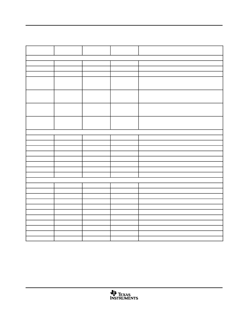
Table 4
7 provides a summary of the McBSP registers.
Table 4
7. McBSP Register Summary
NAME
ADDRESS
0x00 78xxh
TYPE
(R/W)
DATA REGISTERS, RECEIVE, TRANSMIT
0x0000
0x0000
0x0000
RESET VALUE
(HEX)
DESCRIPTION
McBSP Receive Buffer Register
McBSP Receive Shift Register
McBSP Transmit Shift Register
McBSP Data Receive Register 2
Read First if the word size is greater than 16 bits,
else ignore DRR2
DRR2
00
R
0x0000
DRR1
01
R
0x0000
McBSP Data Receive Register 1
Read Second if the word size is greater than 16 bits,
else read DRR1 only
DXR2
02
W
0x0000
McBSP Data Transmit Register 2
Write First if the word size is greater than 16 bits,
else ignore DXR2
DXR1
03
W
0x0000
McBSP Data Transmit Register 1
Write Second if the word size is greater than 16 bits,
else write to DXR1 only
McBSP CONTROL REGISTERS
0x0000
0x0000
0x0000
0x0000
0x0000
0x0000
0x0000
0x0000
MULTICHANNEL CONTROL REGISTERS
R/W
0x0000
R/W
0x0000
R/W
0x0000
R/W
0x0000
R/W
0x0000
R/W
0x0000
R/W
0x0000
R/W
0x0000
R/W
0x0000
R/W
0x0000
R/W
0x0000
SPCR2
SPCR1
RCR2
RCR1
XCR2
XCR1
SRGR2
SRGR1
04
05
06
07
08
09
0A
0B
R/W
R/W
R/W
R/W
R/W
R/W
R/W
R/W
McBSP Serial Port Control Register 2
McBSP Serial Port Control Register 1
McBSP Receive Control Register 2
McBSP Receive Control Register 1
McBSP Transmit Control Register 2
McBSP Transmit Control Register 1
McBSP Sample Rate Generator Register 2
McBSP Sample Rate Generator Register 1
MCR2
MCR1
RCERA
RCERB
XCERA
XCERB
PCR1
RCERC
RCERD
XCERC
XCERD
0C
0D
0E
0F
10
11
12
13
14
15
16
McBSP Multichannel Register 2
McBSP Multichannel Register 1
McBSP Receive Channel Enable Register Partition A
McBSP Receive Channel Enable Register Partition B
McBSP Transmit Channel Enable Register Partition A
McBSP Transmit Channel Enable Register Partition B
McBSP Pin Control Register
McBSP Receive Channel Enable Register Partition C
McBSP Receive Channel Enable Register Partition D
McBSP Transmit Channel Enable Register Partition C
McBSP Transmit Channel Enable Register Partition D
DRR2/DRR1 and DXR2/DXR1 share the same addresses of receive and transmit FIFO registers in FIFO mode.
FIFO pointers advancing is based on order of access to DRR2/DRR1 and DXR2/DXR1 registers.
A
相关PDF资料 |
PDF描述 |
|---|---|
| TMX320F2812PGFS | DIGITAL SIGNAL PROCESSORS |
| TMX320C2811GHHA | TMS320R2811, TMS320R2812 Digital Signal Processors |
| TMX320C2811GHHQ | TMS320R2811, TMS320R2812 Digital Signal Processors |
| TMX320C2811GHHS | TMS320R2811, TMS320R2812 Digital Signal Processors |
| TMX320C2811PBKA | TMS320R2811, TMS320R2812 Digital Signal Processors |
相关代理商/技术参数 |
参数描述 |
|---|---|
| TMX320F2812PBKA | 制造商:TI 制造商全称:Texas Instruments 功能描述:TMS320R2811, TMS320R2812 Digital Signal Processors |
| TMX320F2812PBKQ | 制造商:TI 制造商全称:Texas Instruments 功能描述:TMS320R2811, TMS320R2812 Digital Signal Processors |
| TMX320F2812PBKS | 制造商:TI 制造商全称:Texas Instruments 功能描述:DIGITAL SIGNAL PROCESSORS |
| TMX320F2812PGFA | 制造商:Rochester Electronics LLC 功能描述:- Bulk 制造商:Texas Instruments 功能描述: |
| TMX320F2812PGFMEP | 制造商:TI 制造商全称:Texas Instruments 功能描述:Digital Signal Processors |
发布紧急采购,3分钟左右您将得到回复。