- 您现在的位置:买卖IC网 > PDF目录68419 > TPS5210PWPG4 (TEXAS INSTRUMENTS INC) 2 A SWITCHING CONTROLLER, 200 kHz SWITCHING FREQ-MAX, PDSO28 PDF资料下载
参数资料
| 型号: | TPS5210PWPG4 |
| 厂商: | TEXAS INSTRUMENTS INC |
| 元件分类: | 稳压器 |
| 英文描述: | 2 A SWITCHING CONTROLLER, 200 kHz SWITCHING FREQ-MAX, PDSO28 |
| 封装: | GREEN, PLASTIC, HTSSOP-28 |
| 文件页数: | 23/35页 |
| 文件大小: | 846K |
| 代理商: | TPS5210PWPG4 |
第1页第2页第3页第4页第5页第6页第7页第8页第9页第10页第11页第12页第13页第14页第15页第16页第17页第18页第19页第20页第21页第22页当前第23页第24页第25页第26页第27页第28页第29页第30页第31页第32页第33页第34页第35页
TPS5210
PROGRAMMABLE SYNCHRONOUS BUCK REGULATOR CONTROLLER
SLVS171A SEPTEMBER 1998 REVISED MAY 1999
3
POST OFFICE BOX 655303
DALLAS, TEXAS 75265
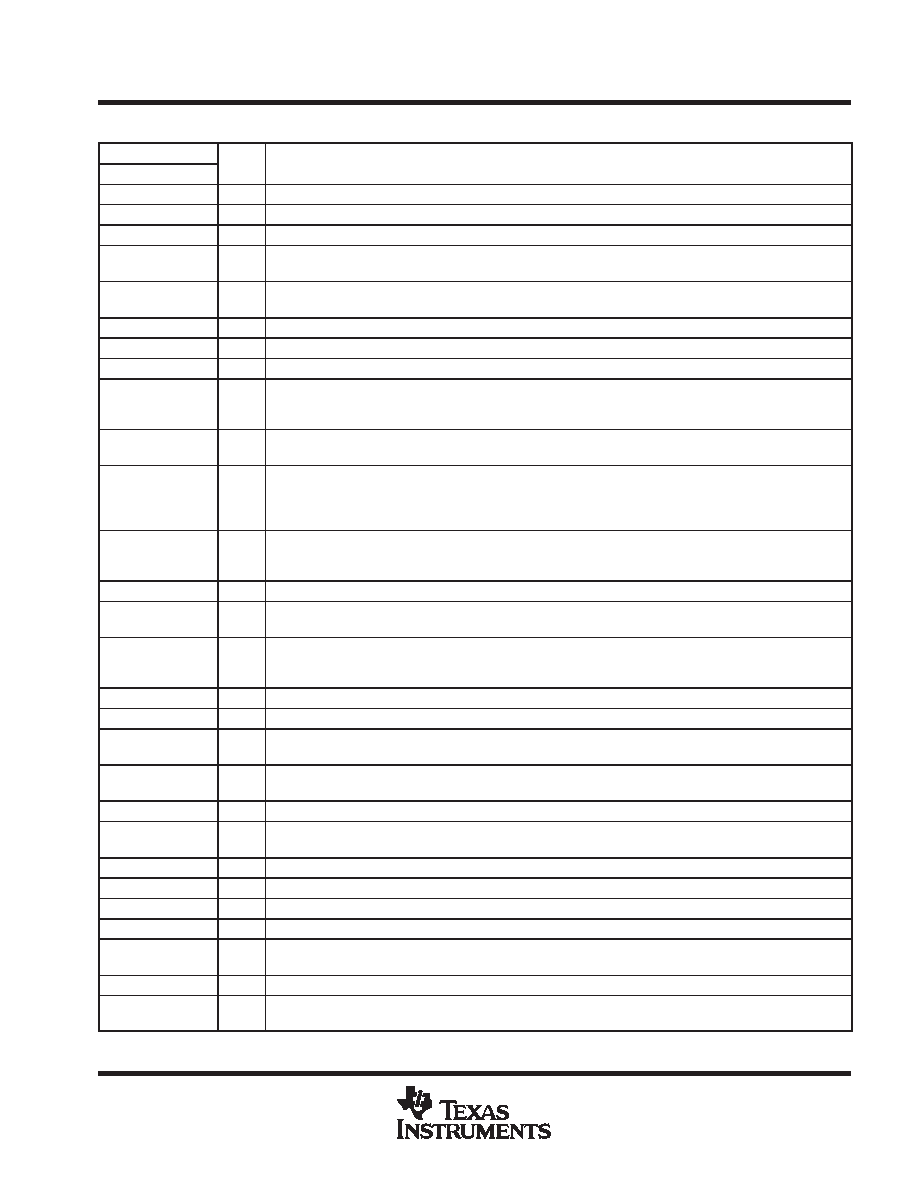
Terminal Functions
TERMINAL
I/O
DESCRIPTION
NAME
NO.
I/O
DESCRIPTION
ANAGND
7
Analog ground
BIAS
9
O
Analog BIAS pin. A 1-
F ceramic capacitor should be connected from BIAS to ANAGND.
BOOT
16
I
Bootstrap. Connect a 1-
F low-ESR capacitor from BOOT to BOOTLO.
BOOTLO
18
O
Bootstrap low. Connect BOOTLO to the junction of the high-side and low-side FETs for floating drive
configuration. Connect BOOTLO to PGND for ground reference drive configuration.
DROOP
2
I
Droop voltage. Voltage input used to set the amount of output-voltage set-point droop as a function of load
current. The amount of droop compensation is set with a resistor divider between IOUT and ANAGND.
DRV
14
O
Drive regulator for the FET drivers. A 1-
F ceramic capacitor should be connected from DRV to DRVGND.
DRVGND
12
Drive ground. Ground for FET drivers. Connect to FET PWRGND.
HIGHDR
17
O
High drive. Output drive to high-side power switching FETs
HISENSE
19
I
High current sense. For current sensing across high-side FETs, connect to the drain of the high-side FETs; for
optional resistor sensing scheme, connect to power supply side of current-sense resistor placed in series with
high-side FET drain.
INHIBIT
22
I
Disables the drive signals to the MOSFET drivers. Can also serve as UVLO for system logic supply (either 3.3 V
or 5 V).
IOUT
1
O
Current out. Output voltage on this pin is proportional to the load current as measured across the Rds(on) of the
high-side FETs. The voltage on this pin equals 2
×Rds(on)×IOUT. In applications where very accurate current
sensing is required, a sense resistor should be connected between the input supply and the drain of the high-side
FETs.
IOUTLO
21
O
Current sense low output. This is the voltage on the LOSENSE pin when the high-side FETs are on. A ceramic
capacitor should be connected from IOUTLO to HISENSE to hold the sensed voltage while the high-side FETs
are off. Capacitance range should be between 0.033
F and 0.1 F.
LODRV
10
I
Low drive enable. Normally tied to 5 V. To activate the low-side FETs as a crowbar, pull LODRV low.
LOHIB
11
I
Low side inhibit. Connect to the junction of the high and low side FETs to control the anti-cross-conduction and
eliminate shoot-through current. Disabled when configured in crowbar mode.
LOSENSE
20
I
Low current sense. For current sensing across high-side FETs, connect to the source of the high-side FETs; for
optional resistor sensing scheme, connect to high-side FET drain side of current-sense resistor placed in series
with high-side FET drain.
LOWDR
13
O
Low drive. Output drive to synchronous rectifier FETs
OCP
3
I
Over current protection. Current limit trip point is set with a resistor divider between IOUT and ANAGND.
PWRGD
28
O
Power good. Power Good signal goes high when output voltage is within 7% of voltage set by VID pins.
Open-drain output.
SLOWST
8
O
Slow Start (soft start). A capacitor from SLOWST to ANAGND sets the slowstart time.
Slowstart current = IVREFB/5
VCC
15
12-V supply. A 1-
F ceramic capacitor should be connected from VCC to DRVGND.
VHYST
4
I
HYSTERESIS set pin. The hysteresis is set with a resistor divider from VREFB to ANAGND.
The hysteresis window = 2
× (VREFB – VHYST)
VID0
27
I
Voltage Identification input 0
VID1
26
I
Voltage Identification input 1
VID2
25
I
Voltage Identification input 2
VID3
24
I
Voltage Identification input 3
VID4
23
I
Voltage Identification input 4. Digital inputs that set the output voltage of the converter. The code pattern for
setting the output voltage is located in Table 1. Internally pulled up to 5 V with a resistor divider biased from VCC.
VREFB
5
O
Buffered reference voltage from VID network
VSENSE
6
I
Voltage sense Input. To be connected to converter output voltage bus to sense and control output voltage. It is
recommended an RC low pass filter be connected at this pin to filter noise.
相关PDF资料 |
PDF描述 |
|---|---|
| TPS5210PWPR | 2 A SWITCHING CONTROLLER, 200 kHz SWITCHING FREQ-MAX, PDSO28 |
| TPS5210PWP | 2 A SWITCHING CONTROLLER, 200 kHz SWITCHING FREQ-MAX, PDSO28 |
| TPS5300DAPR | 3.3 A SWITCHING CONTROLLER, 500 kHz SWITCHING FREQ-MAX, PDSO32 |
| TPS5300DAP | 3.3 A SWITCHING CONTROLLER, 500 kHz SWITCHING FREQ-MAX, PDSO32 |
| TPS5300DAPRG4 | 3.3 A SWITCHING CONTROLLER, 500 kHz SWITCHING FREQ-MAX, PDSO32 |
相关代理商/技术参数 |
参数描述 |
|---|---|
| TPS5210PWPR | 功能描述:DC/DC 开关控制器 Synch Buck Cntrlr Volume Control RoHS:否 制造商:Texas Instruments 输入电压:6 V to 100 V 开关频率: 输出电压:1.215 V to 80 V 输出电流:3.5 A 输出端数量:1 最大工作温度:+ 125 C 安装风格: 封装 / 箱体:CPAK |
| TPS5210PWPRG4 | 功能描述:DC/DC 开关控制器 Synch Buck Cntrlr Volume Control RoHS:否 制造商:Texas Instruments 输入电压:6 V to 100 V 开关频率: 输出电压:1.215 V to 80 V 输出电流:3.5 A 输出端数量:1 最大工作温度:+ 125 C 安装风格: 封装 / 箱体:CPAK |
| TPS5211 | 制造商:TI 制造商全称:Texas Instruments 功能描述:HIGH FREQUENCY PROGRAMMABLE HYSTERETIC REGULATOR CONTROLLER |
| TPS5211PWP | 功能描述:IC REG CTRLR BUCK PWM 28-HTSSOP RoHS:是 类别:集成电路 (IC) >> PMIC - 稳压器 - DC DC 切换控制器 系列:- 标准包装:4,000 系列:- PWM 型:电压模式 输出数:1 频率 - 最大:1.5MHz 占空比:66.7% 电源电压:4.75 V ~ 5.25 V 降压:是 升压:无 回扫:无 反相:无 倍增器:无 除法器:无 Cuk:无 隔离:无 工作温度:-40°C ~ 85°C 封装/外壳:40-VFQFN 裸露焊盘 包装:带卷 (TR) |
| TPS5211PWPR | 制造商:未知厂家 制造商全称:未知厂家 功能描述:Analog IC |
发布紧急采购,3分钟左右您将得到回复。