- 您现在的位置:买卖IC网 > PDF目录98282 > TPS54233DG4 (TEXAS INSTRUMENTS INC) 2 A SWITCHING REGULATOR, 390 kHz SWITCHING FREQ-MAX, PDSO8 PDF资料下载
参数资料
| 型号: | TPS54233DG4 |
| 厂商: | TEXAS INSTRUMENTS INC |
| 元件分类: | 稳压器 |
| 英文描述: | 2 A SWITCHING REGULATOR, 390 kHz SWITCHING FREQ-MAX, PDSO8 |
| 封装: | GREEN, PLASTIC, MS-012AA, SOIC-8 |
| 文件页数: | 25/25页 |
| 文件大小: | 789K |
| 代理商: | TPS54233DG4 |
SLUS859B
– OCTOBER 2008 – REVISED FEBRUARY 2011
CURRENT MODE COMPENSATION DESIGN
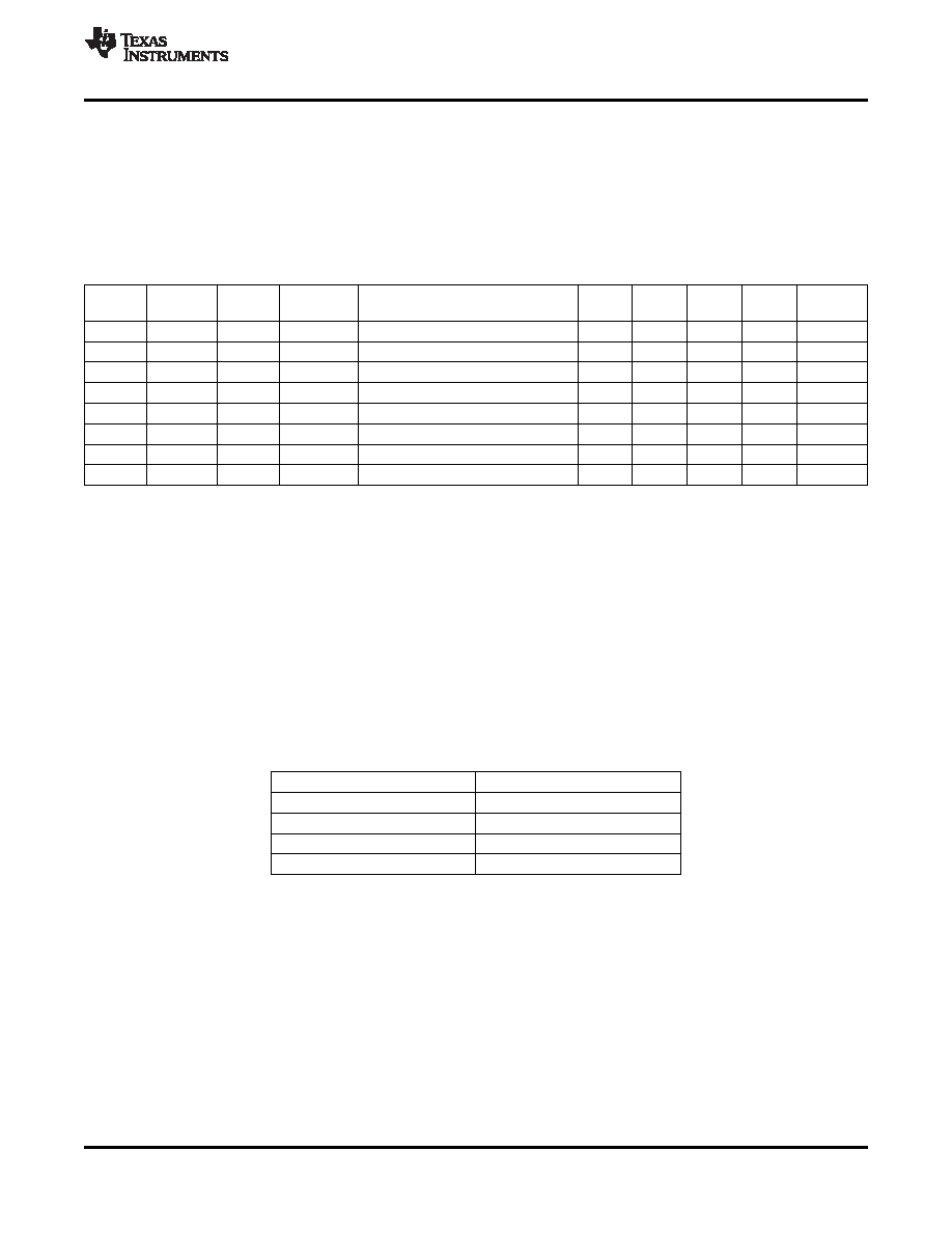
To simplify design efforts using the TPS54233, the typical designs for common applications are listed in Table 1.
For designs using ceramic output capacitors, proper derating of ceramic output capacitance is recommended
when doing the stability analysis. This is because the actual ceramic capacitance drops considerably from the
nominal value when the applied voltage increases. Advanced users may refer to the Step by Step Design
Procedure in the Application Information section for the detailed guidelines or use SwitcherPro
Software tool
Table 1. Typical Designs (Referring to Simplified Schematic on page 1)
VIN
VOUT
Fsw
Lo
Co
RO1
RO2
C2
C1
R3
(V)
(kHz)
(
μH)
(k
)
(k
)
(pF)
(k
)
12
5
300
22
Ceramic 47
μF
10
1.91
68
1800
21
12
3.3
300
15
Ceramic 47
μF
10.2
3.24
47
4700
21
12
1.8
300
10
Ceramic 100
μF x 2
10
8.06
100
4700
21
12
0.9
300
6.8
Ceramic 100
μFx2
10
80.6
100
4700
21
12
5
300
22
Aluminum 330
μF/160 m
10
1.91
56
220
40.2
12
3.3
300
15
Aluminum 470
μF/160 m
10.2
3.24
220
30.9
12
1.8
300
10
SP 220
μF/12 m
10
8.06
100
4700
40.2
12
0.9
300
6.8
SP 220
μF/12 m
10
80.6
100
1800
21
OVERCURRENT PROTECTION AND FREQUENCY SHIFT
The TPS54233 implements current mode control that uses the COMP pin voltage to turn off the high-side
MOSFET on a cycle by cycle basis. Every cycle the switch current and the COMP pin voltage are compared;
when the peak inductor current intersects the COMP pin voltage, the high-side switch is turned off. During
overcurrent conditions that pull the output voltage low, the error amplifier responds by driving the COMP pin high,
causing the switch current to increase. The COMP pin has a maximum clamp internally, which limit the output
current.
The TPS54233 provides robust protection during short circuits. There is potential for overcurrent runaway in the
output inductor during a short circuit at the output. The TPS54233 solves this issue by increasing the off time
during short circuit conditions by lowering the switching frequency. The switching frequency is divided by 8, 4, 2,
and 1 as the voltage ramps from 0 V to 0.8 V on VSENSE pin. The relationship between the switching frequency
and the VSENSE pin voltage is shown in Table 2.
Table 2. Switching Frequency Conditions
SWITCHING FREQUENCY
VSENSE PIN VOLTAGE
300 kHz
VSENSE
≥ 0.6 V
300 kHz / 2
0.6 V
> VSENSE ≥ 0.4 V
300 kHz / 4
0.4 V
> VSENSE ≥ 0.2 V
300 kHz / 8
0.2 V
> VSENSE
OVERVOLTAGE TRANSIENT PROTECTION
The TPS54233 incorporates an overvoltage transient protection (OVTP) circuit to minimize output voltage
overshoot when recovering from output fault conditions or strong unload transients. The OVTP circuit includes an
overvoltage comparator to compare the VSENSE pin voltage and internal thresholds. When the VSENSE pin
voltage goes above 109%
× Vref, the high-side MOSFET will be forced off. When the VSENSE pin voltage falls
below 107%
× Vref, the high-side MOSFET will be enabled again.
THERMAL SHUTDOWN
The device implements an internal thermal shutdown to protect itself if the junction temperature exceeds 165
°C.
The thermal shutdown forces the device to stop switching when the junction temperature exceeds the thermal
trip threshold. Once the die temperature decreases below 165
°C, the device reinitiates the power up sequence.
2008–2011, Texas Instruments Incorporated
9
Product Folder Link(s): TPS54233
相关PDF资料 |
PDF描述 |
|---|---|
| TPS54240QDGQRQ1 | 2.5 A SWITCHING REGULATOR, 2500 kHz SWITCHING FREQ-MAX, PDSO10 |
| TPS54260DGQR | SWITCHING REGULATOR, 2500 kHz SWITCHING FREQ-MAX, PDSO10 |
| TPS54260QDGQRQ1 | 2.5 A SWITCHING REGULATOR, 2500 kHz SWITCHING FREQ-MAX, PDSO10 |
| TPS5430MDDAREPG4 | 8.5 A SWITCHING REGULATOR, 600 kHz SWITCHING FREQ-MAX, PDSO8 |
| TPS54310MPWPREP | 6 A SWITCHING REGULATOR, 775 kHz SWITCHING FREQ-MAX, PDSO20 |
相关代理商/技术参数 |
参数描述 |
|---|---|
| TPS54233DR | 功能描述:直流/直流开关转换器 28V,2A,300khZ Non- synch Buck RoHS:否 制造商:STMicroelectronics 最大输入电压:4.5 V 开关频率:1.5 MHz 输出电压:4.6 V 输出电流:250 mA 输出端数量:2 最大工作温度:+ 85 C 安装风格:SMD/SMT |
| TPS54233DRG4 | 功能描述:直流/直流开关转换器 28V,2A,300khZ Non- Synch Buck RoHS:否 制造商:STMicroelectronics 最大输入电压:4.5 V 开关频率:1.5 MHz 输出电压:4.6 V 输出电流:250 mA 输出端数量:2 最大工作温度:+ 85 C 安装风格:SMD/SMT |
| TPS54233EVM-373 | 功能描述:电源管理IC开发工具 TPS54233EVM-373 Eval Mod RoHS:否 制造商:Maxim Integrated 产品:Evaluation Kits 类型:Battery Management 工具用于评估:MAX17710GB 输入电压: 输出电压:1.8 V |
| TPS54233-Q1 | 制造商:TI 制造商全称:Texas Instruments 功能描述:2-A, 28-V INPUT, STEP-DOWN DC/DC CONVERTER WITH ECO-MODEa?¢ |
| TPS54233QDRQ1 | 功能描述:开关变换器、稳压器与控制器 AC 3.5-28Vin,2A 300kHz SD Converter RoHS:否 制造商:Texas Instruments 输出电压:1.2 V to 10 V 输出电流:300 mA 输出功率: 输入电压:3 V to 17 V 开关频率:1 MHz 工作温度范围: 安装风格:SMD/SMT 封装 / 箱体:WSON-8 封装:Reel |
发布紧急采购,3分钟左右您将得到回复。