- 您现在的位置:买卖IC网 > PDF目录199556 > UDA1345TS/N2,118 (NXP SEMICONDUCTORS) Economy audio CODEC; Package: SOT341-1 (SSOP28); Container: Reel Pack, SMD, 13" PDF资料下载
参数资料
| 型号: | UDA1345TS/N2,118 |
| 厂商: | NXP SEMICONDUCTORS |
| 元件分类: | 消费家电 |
| 英文描述: | Economy audio CODEC; Package: SOT341-1 (SSOP28); Container: Reel Pack, SMD, 13" |
| 中文描述: | SPECIALTY CONSUMER CIRCUIT, PDSO28 |
| 封装: | 5.30 MM, PLASTIC, SSOP-28 |
| 文件页数: | 27/28页 |
| 文件大小: | 136K |
| 代理商: | UDA1345TS/N2,118 |
第1页第2页第3页第4页第5页第6页第7页第8页第9页第10页第11页第12页第13页第14页第15页第16页第17页第18页第19页第20页第21页第22页第23页第24页第25页第26页当前第27页第28页
2002 May 28
8
Philips Semiconductors
Product specication
Economy audio CODEC
UDA1345TS
7
FUNCTIONAL DESCRIPTION
The UDA1345TS accommodates slave mode only, this
means that in all applications the system devices must
provide the system clocks (being the system clock itself
and the digital audio interface signals).
The system clock must be locked in frequency to the audio
digital interface input signals.
The BCK clock can be up to 128fs, or in other words the
BCK frequency is 128 times the Word Select (WS)
frequency or less: fBCK ≤ 128 × fWS.
Important: the WS edge MUST fall on the negative edge
of the BCK at all times for proper operation of the digital I/O
data interface.
Note: the sampling frequency range is from 8 to 100 kHz,
however for the 512fs clock mode the sampling range is
from 8 to 55 kHz.
7.1
Analog-to-Digital Converter (ADC)
The stereo ADC of the UDA1345TS consists of two
5th-order Sigma-Delta modulators. They have a modified
Ritchie-coder architecture in a differential switched
capacitor implementation. The oversampling ratio is 64.
7.2
Analog front-end
The analog front-end is equipped with a selectable 0 dB or
6 dB gain block (the pin to select this mode is given in
Section 7.10). This block can be used in applications in
which both 1 V (RMS) and 2 V (RMS) input signals can be
input to the UDA1345TS.
In applications in which a 2 V (RMS) input signal is used,
a12 k
resistor must be used in series with the input of the
ADC. This forms a voltage divider together with the internal
ADC resistor and ensures that only 1 V (RMS) maximum
is input to the IC. Using this application for a 2 V (RMS)
input signal, the switch must be set to 0 dB. When a
1 V (RMS) input signal is input to the ADC in the same
application, the gain switch must be set to 6 dB.
An overview of the maximum input voltages allowed
against the presence of an external resistor and the setting
of the gain switch is given in Table 1; the power supply
voltage is assumed to be 3 V.
Table 1
Application modes using input gain stage
7.3
Decimation lter (ADC)
The decimation from 64fs to 1fs is performed in two stages.
The first stage realizes a 4th-order
characteristic.
This filter decreases the sample rate by 8. The second
stage consists of 2 half-band filters and a recursive filter,
each decimating by a factor of 2.
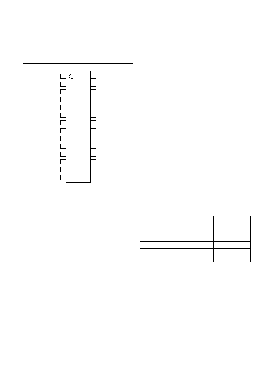
handbook, halfpage
VSSA(ADC)
VDDA(ADC)
VINL
Vref(A)
VINR
VADCN
VADCP
MC1
MP1
VDDD
VSSD
SYSCLK
MP2
MP3
Vref(D)
VSSO
VOUTL
VDDO
VDDA(DAC)
VSSA(DAC)
VOUTR
MC2
MP5
DATAI
DATAO
WS
BCK
MP4
1
2
3
4
5
6
7
8
9
10
11
12
13
28
27
26
25
24
23
22
21
20
19
18
17
16
15
14
UDA1345TS
MGS876
Fig.2 Pin configuration.
RESISTOR
(12 k
)
INPUT GAIN
SWITCH
MAXIMUM
INPUT
VOLTAGE
Present
0 dB
2 V (RMS)
Present
6 dB
1 V (RMS)
Absent
0 dB
1 V (RMS)
Absent
6 dB
0.5 V (RMS)
sin x
x
------------
相关PDF资料 |
PDF描述 |
|---|---|
| UDA1345TS/N2,112 | Economy audio CODEC; Package: SOT341-1 (SSOP28); Container: Tube |
| UDA1361TS/N1,112 | 96 kHz sampling 24-bit stereo audio ADC; Package: SOT369-1 (SSOP16); Container: Tube |
| UDA1361TS/N1,118 | 96 kHz sampling 24-bit stereo audio ADC; Package: SOT369-1 (SSOP16); Container: Reel Pack, SMD, 13" |
| UDA1380HN/N2,118 | Stereo audio coder-decoder for MD, CD and MP3; Package: SOT617-1 (HVQFN32); Container: Reel Pack, SMD, 13" |
| UDA1380TT | Stereo audio coder-decoder for MD, CD and MP3 |
相关代理商/技术参数 |
参数描述 |
|---|---|
| UDA1350AH | 制造商:PHILIPS 制造商全称:NXP Semiconductors 功能描述:IEC 958 audio DAC |
| UDA1350ATS | 制造商:PHILIPS 制造商全称:NXP Semiconductors 功能描述:IEC 958 audio DAC |
| UDA1351 | 制造商:PHILIPS 制造商全称:NXP Semiconductors 功能描述:96 kHz IEC 958 audio DAC |
| UDA1351H | 制造商:PHILIPS 制造商全称:NXP Semiconductors 功能描述:96 kHz IEC 958 audio DAC |
| UDA1351H/N1,551 | 功能描述:数模转换器- DAC 96 KHZ SPDIF DAC RoHS:否 制造商:Texas Instruments 转换器数量:1 DAC 输出端数量:1 转换速率:2 MSPs 分辨率:16 bit 接口类型:QSPI, SPI, Serial (3-Wire, Microwire) 稳定时间:1 us 最大工作温度:+ 85 C 安装风格:SMD/SMT 封装 / 箱体:SOIC-14 封装:Tube |
发布紧急采购,3分钟左右您将得到回复。