- 您现在的位置:买卖IC网 > Datasheet目录529 > UPA611TA-T2-A (Renesas Electronics America)MOSFET N-CH DUAL 30V SC74-6 Datasheet资料下载
参数资料
| 型号: | UPA611TA-T2-A |
| 厂商: | Renesas Electronics America |
| 文件页数: | 3/7页 |
| 文件大小: | 0K |
| 描述: | MOSFET N-CH DUAL 30V SC74-6 |
| 标准包装: | 3,000 |
| FET 型: | 2 个 N 沟道(双) |
| FET 特点: | 逻辑电平门 |
| 漏极至源极电压(Vdss): | 30V |
| 电流 - 连续漏极(Id) @ 25° C: | 100mA |
| 开态Rds(最大)@ Id, Vgs @ 25° C: | 5 欧姆 @ 10mA,10V |
| 输入电容 (Ciss) @ Vds: | 9pF @ 3V |
| 功率 - 最大: | 300mW |
| 安装类型: | 表面贴装 |
| 封装/外壳: | SC-74,SOT-457 |
| 供应商设备封装: | SC-74-6,(迷你型) |
| 包装: | 带卷 (TR) |
�� ��
��
��DATA� SHEET�
�MOS� FIELD� EFFECT� TRANSISTOR�
�μ� PA611TA�
�N-CHANNEL� MOS� FIELD� EFFECT� TRANSISTOR�
�FOR� HIGH� SPEED� SWITCHING�
�DESCRIPTION�
�The� μ� PA611TA� is� a� switching� device� which� can� be� driven� directly� by� a�
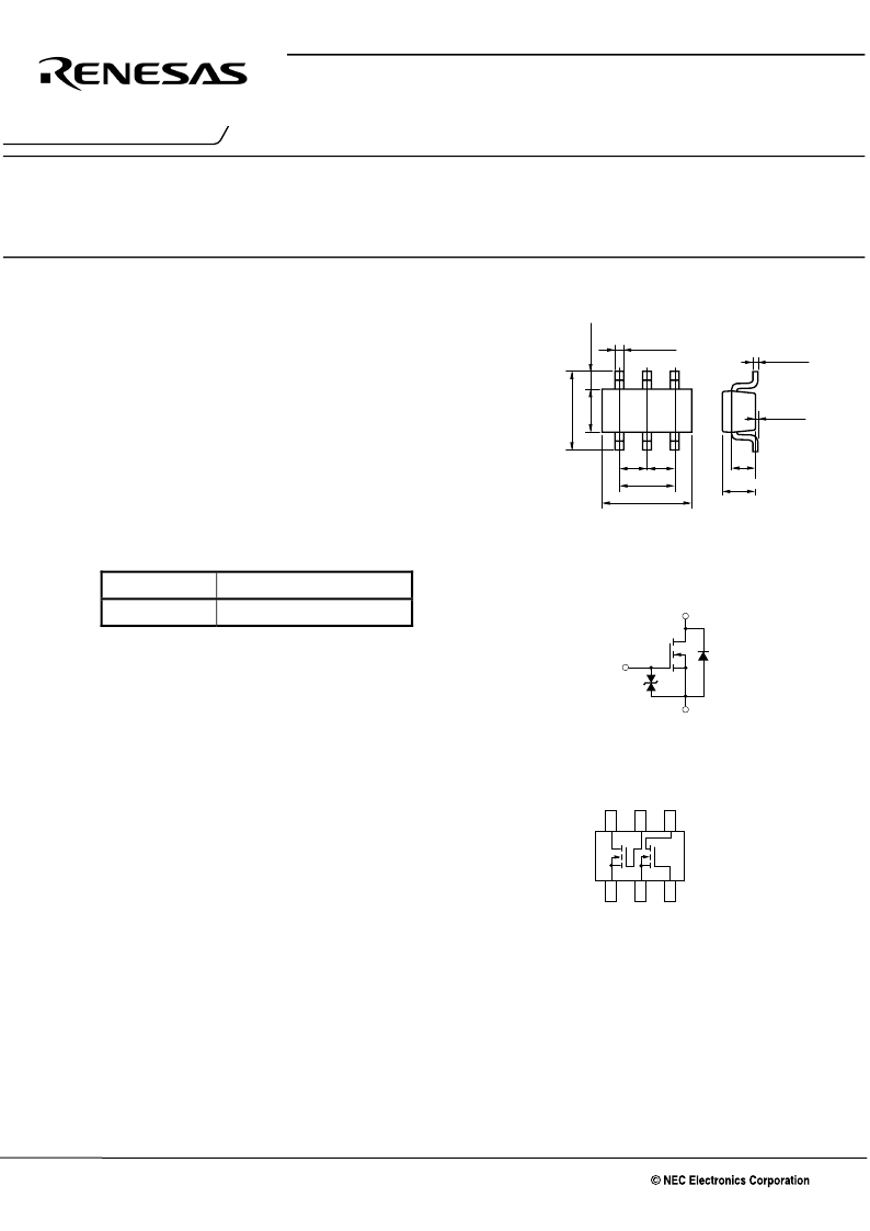
�PACKAGE� DRAWING� (Unit� :� mm)�
�2.5-V� power� source.�
�The� μ� PA611TA� has� excellent� switching� characteristics,� and� is� suitable� for�
�+0.1�
�0.32� –0.05�
�+0.1�
�0.16� –0.06�
�use� as� a� high-speed� switching� device� in� digital� circuits.�
�0� to� 0.1�
�FEATURES�
�?� Can� be� driven� by� a� 2.5-V� power� source�
�?� Low� gate� cut-off� voltage�
�0.95� 0.95�
�1.9�
�2.9� ±0.2�
�0.8�
�1.1 to� 1.4�
�ORDERING� INFORMATION�
�PART� NUMBER�
�PACKAGE�
�EQUIVALENT� CIRCUIT�
�(1/2� Circuit)�
�μ� PA611TA�
�SC-74� (Mini� Mold)�
�Gate�
�Drain�
�Internal�
�Diode�
�ABSOLUTE� MAXIMUM� RATINGS� (T� A� =� 25°C)�
�Gate�
�Drain� to� Source� Voltage�
�Gate� to� Source� Voltage�
�V� DSS�
�V� GSS�
�30�
�±20�
�V�
�V�
�Protection�
�Diode�
�Source�
�Drain� Current� (DC)�
�I� D(DC)�
�±0.1�
�A�
�PIN� CONNECTION� (Top� View)�
�Drain� Current� (pulse)�
�Note�
�I� D(pulse)�
�±0.4�
�A�
�Total� Power� Dissipation�
�Channel� Temperature�
�Storage� Temperature�
�P� T�
�T� ch�
�T� stg�
�300� (TOTAL)�
�150�
�–55� to� +150�
�mW�
�°C�
�°C�
�6�
�5�
�4�
�1.� Source� 1�
�2.� Source� 2�
�3.� Gate� 2�
�4.� Drain� 2�
�Note� PW� ≤� 10� μ� s,� Duty� Cycle� ≤� 1� %�
�1�
�2�
�3�
�5.� Gate� 1�
�6.� Drain� 1�
�Marking� :� IB�
�Remark�
�The� diode� connected� between� the� gate� and� source� of� the� transistor� serves� as� a� protector� against� ESD.�
�When� this� device� actually� used,� an� additional� protection� circuit� is� externally� required� if� a� voltage� exceeding�
�the� rated� voltage� may� be� applied� to� this� device.�
�The� information� in� this� document� is� subject� to� change� without� notice.� Before� using� this� document,� please�
�confirm� that� this� is� the� latest� version.�
�Not� all� products� and/or� types� are� available� in� every� country.� Please� check� with� an� NEC� Electronics�
�sales� representative� for� availability� and� additional� information.�
�Document� No.� D11707EJ2V0DS00� (2nd� edition)�
�Date� Published� September� 2006� NS� CP(K)�
�Printed� in� Japan�
�The� mark� <R>� shows� major� revised� points.�
�1999�
�The� revised� points� can� be� easily� searched� by� copying� an� "<R>"� in� the� PDF� file� and� specifying� it� in� the� "Find� what:"� field.�
�相关PDF资料 |
PDF描述 |
|---|---|
| UPA621TT-E2-A | MOSFET N-CH 20V 6-WSOF |
| UPA622TT-E2-A | MOSFET N-CH 30V 6-WSOF |
| UPA650TT-E1-A | MOSFET P-CH 12V 6-WSOF |
| UPA672T-T2-A | MOSFET N-CH DUAL 50V SC-70 |
| UPA675T-T2-A | MOSFET N-CH DUAL 16V SC-70 |
相关代理商/技术参数 |
参数描述 |
|---|---|
| UPA620 | 制造商:未知厂家 制造商全称:未知厂家 功能描述:UPA620TT Data Sheet | Data Sheet[09/2002] |
| UPA620TT | 制造商:NEC 制造商全称:NEC 功能描述:N-CHANNEL MOS FIELD EFFECT TRANSISTOR FOR SWITCHING |
| UPA621 | 制造商:未知厂家 制造商全称:未知厂家 功能描述:UPA621TT Data Sheet | Data Sheet[06/2002] |
| UPA621TT | 制造商:NEC 制造商全称:NEC 功能描述:N-CHANNEL MOS FIELD EFFECT TRANSISTOR FOR SWITCHING |
| UPA621TT-E1-A | 功能描述:MOSFET N-CH 20V 6-WSOF RoHS:是 类别:分离式半导体产品 >> FET - 单 系列:- 标准包装:1,000 系列:MESH OVERLAY™ FET 型:MOSFET N 通道,金属氧化物 FET 特点:逻辑电平门 漏极至源极电压(Vdss):200V 电流 - 连续漏极(Id) @ 25° C:18A 开态Rds(最大)@ Id, Vgs @ 25° C:180 毫欧 @ 9A,10V Id 时的 Vgs(th)(最大):4V @ 250µA 闸电荷(Qg) @ Vgs:72nC @ 10V 输入电容 (Ciss) @ Vds:1560pF @ 25V 功率 - 最大:40W 安装类型:通孔 封装/外壳:TO-220-3 整包 供应商设备封装:TO-220FP 包装:管件 |
发布紧急采购,3分钟左右您将得到回复。