- 您现在的位置:买卖IC网 > PDF目录11181 > UPD78F9502MA-CAC-A (Renesas Electronics America)MCU 8BIT SGL CHIP PDF资料下载
参数资料
| 型号: | UPD78F9502MA-CAC-A |
| 厂商: | Renesas Electronics America |
| 文件页数: | 49/158页 |
| 文件大小: | 0K |
| 描述: | MCU 8BIT SGL CHIP |
| 标准包装: | 400 |
| 系列: | 78K0S/Kx1+ |
| 核心处理器: | 78K0S |
| 芯体尺寸: | 8-位 |
| 速度: | 10MHz |
| 外围设备: | LVD,POR,PWM,WDT |
| 输入/输出数: | 7 |
| 程序存储器容量: | 4KB(4K x 8) |
| 程序存储器类型: | 闪存 |
| RAM 容量: | 128 x 8 |
| 电压 - 电源 (Vcc/Vdd): | 2 V ~ 5.5 V |
| 振荡器型: | 内部 |
| 工作温度: | -40°C ~ 85°C |
| 封装/外壳: | 10-LSSOP(0.225",5.72mm 宽) |
| 包装: | 托盘 |
第1页第2页第3页第4页第5页第6页第7页第8页第9页第10页第11页第12页第13页第14页第15页第16页第17页第18页第19页第20页第21页第22页第23页第24页第25页第26页第27页第28页第29页第30页第31页第32页第33页第34页第35页第36页第37页第38页第39页第40页第41页第42页第43页第44页第45页第46页第47页第48页当前第49页第50页第51页第52页第53页第54页第55页第56页第57页第58页第59页第60页第61页第62页第63页第64页第65页第66页第67页第68页第69页第70页第71页第72页第73页第74页第75页第76页第77页第78页第79页第80页第81页第82页第83页第84页第85页第86页第87页第88页第89页第90页第91页第92页第93页第94页第95页第96页第97页第98页第99页第100页第101页第102页第103页第104页第105页第106页第107页第108页第109页第110页第111页第112页第113页第114页第115页第116页第117页第118页第119页第120页第121页第122页第123页第124页第125页第126页第127页第128页第129页第130页第131页第132页第133页第134页第135页第136页第137页第138页第139页第140页第141页第142页第143页第144页第145页第146页第147页第148页第149页第150页第151页第152页第153页第154页第155页第156页第157页第158页
CHAPTER 7 8-BIT TIMER H1
User’s Manual U18172EJ3V0UD
140
7.4.2
Operation as PWM output mode
In PWM output mode, a pulse with an arbitrary duty and arbitrary cycle can be output.
8-bit timer compare register 01 (CMP01) controls the cycle of timer output (TOH1). Rewriting the CMP01 register
during timer operation is prohibited.
8-bit timer compare register 11 (CMP11) controls the duty of timer output (TOH1). Rewriting the CMP11 register
during timer operation is possible.
The operation in PWM output mode is as follows.
TOH1 output becomes active and 8-bit timer counter H1 is cleared to 0 when 8-bit timer counter H1 and the
CMP01 register match after the timer count is started. TOH1 output becomes inactive when 8-bit timer counter H1
and the CMP11 register match.
(1) Usage
In PWM output mode, a pulse for which an arbitrary duty and arbitrary cycle can be set is output.
<1>
Set each register.
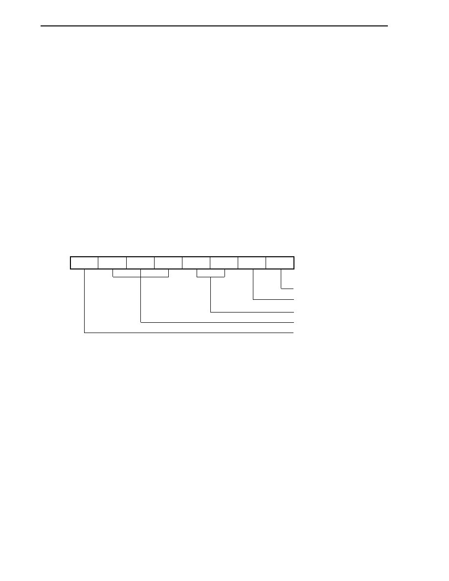
Figure 7-9. Register Setting in PWM Output Mode
(i)
Setting timer H mode register 1 (TMHMD1)
0
0/1
1
0
0/1
1
TMMD10 TOLEV1
TOEN1
CKS11
CKS12
TMHE1
TMHMD1
CKS10
TMMD11
Timer output enabled
Timer output level inversion setting
PWM output mode selection
Count clock (fCNT) selection
Count operation stopped
(ii) Setting CMP01 register
Compare value (N): Cycle setting
(iii) Setting CMP11 register
Compare value (M): Duty setting
Remark
00H
≤ CMP11 (M) < CMP01 (N) ≤ FFH
<2>
The count operation starts when TMHE1 = 1.
<3>
The CMP01 register is the compare register that is to be compared first after count operation is enabled.
When the values of 8-bit timer counter H1 and the CMP01 register match, 8-bit timer counter H1 is cleared,
an interrupt request signal (INTTMH1) is generated, and TOH1 output becomes active. At the same time,
the compare register to be compared with 8-bit timer counter H1 is changed from the CMP01 register to the
CMP11 register.
相关PDF资料 |
PDF描述 |
|---|---|
| VE-BNJ-IW-F2 | CONVERTER MOD DC/DC 36V 100W |
| VE-BNJ-IW-F1 | CONVERTER MOD DC/DC 36V 100W |
| VE-BNH-IX-F4 | CONVERTER MOD DC/DC 52V 75W |
| VE-BNP-IW-F4 | CONVERTER MOD DC/DC 13.8V 100W |
| VE-BNP-IW-F2 | CONVERTER MOD DC/DC 13.8V 100W |
相关代理商/技术参数 |
参数描述 |
|---|---|
| UPD78F9510GR-JJG-A | 功能描述:MCU 8BIT SGL CHIP 16PIN RoHS:是 类别:集成电路 (IC) >> 嵌入式 - 微控制器, 系列:78K0S/Kx1+ 标准包装:38 系列:Encore!® XP® 核心处理器:eZ8 芯体尺寸:8-位 速度:5MHz 连通性:IrDA,UART/USART 外围设备:欠压检测/复位,LED,POR,PWM,WDT 输入/输出数:16 程序存储器容量:4KB(4K x 8) 程序存储器类型:闪存 EEPROM 大小:- RAM 容量:1K x 8 电压 - 电源 (Vcc/Vdd):2.7 V ~ 3.6 V 数据转换器:- 振荡器型:内部 工作温度:-40°C ~ 105°C 封装/外壳:20-SOIC(0.295",7.50mm 宽) 包装:管件 其它名称:269-4116Z8F0413SH005EG-ND |
| UPD78F9511GR-JJG-A | 功能描述:MCU 8BIT SGL CHIP 16PIN RoHS:是 类别:集成电路 (IC) >> 嵌入式 - 微控制器, 系列:78K0S/Kx1+ 标准包装:38 系列:Encore!® XP® 核心处理器:eZ8 芯体尺寸:8-位 速度:5MHz 连通性:IrDA,UART/USART 外围设备:欠压检测/复位,LED,POR,PWM,WDT 输入/输出数:16 程序存储器容量:4KB(4K x 8) 程序存储器类型:闪存 EEPROM 大小:- RAM 容量:1K x 8 电压 - 电源 (Vcc/Vdd):2.7 V ~ 3.6 V 数据转换器:- 振荡器型:内部 工作温度:-40°C ~ 105°C 封装/外壳:20-SOIC(0.295",7.50mm 宽) 包装:管件 其它名称:269-4116Z8F0413SH005EG-ND |
| UPD78F9512GR-JJG-A | 功能描述:MCU 8BIT SGL CHIP 16PIN RoHS:是 类别:集成电路 (IC) >> 嵌入式 - 微控制器, 系列:78K0S/Kx1+ 标准包装:38 系列:Encore!® XP® 核心处理器:eZ8 芯体尺寸:8-位 速度:5MHz 连通性:IrDA,UART/USART 外围设备:欠压检测/复位,LED,POR,PWM,WDT 输入/输出数:16 程序存储器容量:4KB(4K x 8) 程序存储器类型:闪存 EEPROM 大小:- RAM 容量:1K x 8 电压 - 电源 (Vcc/Vdd):2.7 V ~ 3.6 V 数据转换器:- 振荡器型:内部 工作温度:-40°C ~ 105°C 封装/外壳:20-SOIC(0.295",7.50mm 宽) 包装:管件 其它名称:269-4116Z8F0413SH005EG-ND |
| UPD78F9801GB-8ES-A | 制造商:Renesas Electronics Corporation 功能描述: |
| UPD78F9842GB-8ES | 制造商:Renesas Electronics Corporation 功能描述: |
发布紧急采购,3分钟左右您将得到回复。