- 您现在的位置:买卖IC网 > PDF目录361590 > UPSD3233A-40T6T (意法半导体) CABLE ASSEMBLY; LEAD-FREE SOLDER; C MALE TO C MALE; 75 OHM, RG59B/U COAX PDF资料下载
参数资料
| 型号: | UPSD3233A-40T6T |
| 厂商: | 意法半导体 |
| 英文描述: | CABLE ASSEMBLY; LEAD-FREE SOLDER; C MALE TO C MALE; 75 OHM, RG59B/U COAX |
| 中文描述: | 闪存可编程系统设备与8032微控制器核心和64Kbit SRAM的 |
| 文件页数: | 88/176页 |
| 文件大小: | 1081K |
| 代理商: | UPSD3233A-40T6T |
第1页第2页第3页第4页第5页第6页第7页第8页第9页第10页第11页第12页第13页第14页第15页第16页第17页第18页第19页第20页第21页第22页第23页第24页第25页第26页第27页第28页第29页第30页第31页第32页第33页第34页第35页第36页第37页第38页第39页第40页第41页第42页第43页第44页第45页第46页第47页第48页第49页第50页第51页第52页第53页第54页第55页第56页第57页第58页第59页第60页第61页第62页第63页第64页第65页第66页第67页第68页第69页第70页第71页第72页第73页第74页第75页第76页第77页第78页第79页第80页第81页第82页第83页第84页第85页第86页第87页当前第88页第89页第90页第91页第92页第93页第94页第95页第96页第97页第98页第99页第100页第101页第102页第103页第104页第105页第106页第107页第108页第109页第110页第111页第112页第113页第114页第115页第116页第117页第118页第119页第120页第121页第122页第123页第124页第125页第126页第127页第128页第129页第130页第131页第132页第133页第134页第135页第136页第137页第138页第139页第140页第141页第142页第143页第144页第145页第146页第147页第148页第149页第150页第151页第152页第153页第154页第155页第156页第157页第158页第159页第160页第161页第162页第163页第164页第165页第166页第167页第168页第169页第170页第171页第172页第173页第174页第175页第176页
μ
PSD323X
88/176
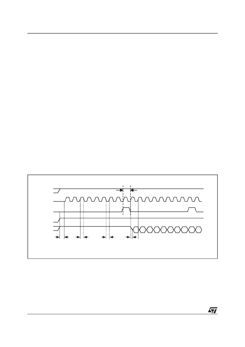
DDC1 Protocol
DDC1 is primitive and a point to point interface.
The monitoris always putat “Transmit only” mode.
In the initialization phase, 9 clock cycles on V
CLK
pin will be given for the internal synchronization.
During this period,the SDA pin will be kept at high
impedance state.
If DDC1 hardwaremode is used, the following pro-
cedure is recommended to proceed DDC1 opera-
tion.
1. Reset DDC1enable (bydefault, DDC1 enableis
cleared as LOW after Power-on Reset).
2. Set SWENB as high (the default value is zero.)
3. Depending on the data size of EDID data, set
EX_DAT as LOW (128 bytes) or HIGH (256
bytes).
4. By using bulky moving commands (DDCADR,
RAMBUF involved) to move the entire EDID
data to RAM buffer.
5. Reset SWENB to LOW.
6. Reset DDCADR to 00h.
7. Set DDC1 enable as HIGH.
In case SWENB is set as high, interrupt service
routine is finished within 133 machine cycle in
40MHz System clock.
The maximum V
SYNC
(V
CLK
) frequency is 25Khz
(40
μ
s). And the 9th clock of V
SYNC
(V
CLK
) is inter-
rupt period.
So the machine cycle be needed is calculated as
below. For example,
When 40MHz system clock, 40
μ
s = 133 x (25ns x
12); 133 machine cycle.
12MHz system clock, 40
μ
s = 40 x (83.3ns x 12);
40 machine cycle.
8MHz system clock, 40
μ
s = 26 x (125ns x 12); 26
machine cycle.
Note:
If EX_DAT equals to LOW, it is meant the
lower part is occupied by DDC1 operation and the
upper part is still free to the system. Nevertheless,
the effect of the post increment just applies to the
part related to DDC1operation. In other words,the
system program is still able to address the loca-
tions from 128 to 255 in the RAM buffer through
MOVX command but without thefacility of the post
increment. For example, the case of accessing
200 of the RAM Buffer:
MOV R0, #200, and
MOVX A, @R0
Figure 42. Transmission Protocol in the DDC1 Interface
AI06652
1
2
3
4
5
6
7
8
9
1
2
3
4
5
6
7
8
9
1
B
tSU(DDC1)
tDOV
Hi-Z
SC
VCLK
DDC1INT
DDC1EN
SD
tH(VCLK)
tL(VCLK)
Max=40us
B
B
B
B
B
B
B
B
HiZ
相关PDF资料 |
PDF描述 |
|---|---|
| UPSD3233A-40U6T | Flash Programmable System Devices with 8032 Microcontroller Core and 64Kbit SRAM |
| UPSD3233AV-24T1T | Flash Programmable System Devices with 8032 Microcontroller Core and 64Kbit SRAM |
| UPSD3233AV-24T6T | Flash Programmable System Devices with 8032 Microcontroller Core and 64Kbit SRAM |
| UPSD3233BV-40T1T | Flash Programmable System Devices with 8032 Microcontroller Core and 64Kbit SRAM |
| UPSD3233BV-40U6T | Flash Programmable System Devices with 8032 Microcontroller Core and 64Kbit SRAM |
相关代理商/技术参数 |
参数描述 |
|---|---|
| UPSD3233A-40U1 | 制造商:STMICROELECTRONICS 制造商全称:STMicroelectronics 功能描述:Flash Programmable System Device with 8032 Microcontroller Core |
| UPSD3233A-40U1T | 制造商:STMICROELECTRONICS 制造商全称:STMicroelectronics 功能描述:Flash Programmable System Device with 8032 Microcontroller Core |
| UPSD3233A-40U6 | 制造商:STMICROELECTRONICS 制造商全称:STMicroelectronics 功能描述:Flash Programmable System Device with 8032 Microcontroller Core |
| UPSD3233A-40U6T | 制造商:STMICROELECTRONICS 制造商全称:STMicroelectronics 功能描述:Flash Programmable System Devices with 8032 Microcontroller Core |
| UPSD3233AV-24T1 | 制造商:STMICROELECTRONICS 制造商全称:STMicroelectronics 功能描述:Flash Programmable System Device with 8032 Microcontroller Core |
发布紧急采购,3分钟左右您将得到回复。