- 您现在的位置:买卖IC网 > PDF目录275205 > V54C3128164VBC7PC (PROMOS TECHNOLOGIES INC) 8M X 16 SYNCHRONOUS DRAM, 5.4 ns, PBGA54 PDF资料下载
参数资料
| 型号: | V54C3128164VBC7PC |
| 厂商: | PROMOS TECHNOLOGIES INC |
| 元件分类: | DRAM |
| 英文描述: | 8M X 16 SYNCHRONOUS DRAM, 5.4 ns, PBGA54 |
| 封装: | MO-210, FBGA-54 |
| 文件页数: | 9/56页 |
| 文件大小: | 734K |
| 代理商: | V54C3128164VBC7PC |
第1页第2页第3页第4页第5页第6页第7页第8页当前第9页第10页第11页第12页第13页第14页第15页第16页第17页第18页第19页第20页第21页第22页第23页第24页第25页第26页第27页第28页第29页第30页第31页第32页第33页第34页第35页第36页第37页第38页第39页第40页第41页第42页第43页第44页第45页第46页第47页第48页第49页第50页第51页第52页第53页第54页第55页第56页
17
V54C3128(16/80/40)4VB Rev. 1.5 March 2006
ProMOS TECHNOLOGIES
V54C3128(16/80/40)4VB
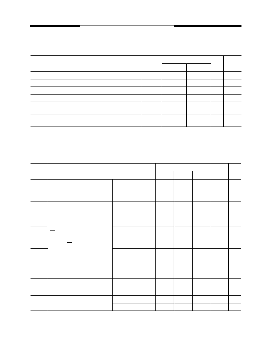
Recommended Operation and Characteristics for LV-TTL
TA = 0 to 70 °C; VSS = 0 V; VCC,VCCQ = 3.3 V ± 0.3 V
Note:
1.
All voltages are referenced to VSS.
2.
VIH may overshoot to VCC + 2.0 V for pulse width of < 4ns with 3.3V. VIL may undershoot to -2.0 V for pulse width < 4.0 ns with
3.3V. Pulse width measured at 50% points with amplitude measured peak to DC reference.
Operating Currents (TA = 0 to 70°C, VCC = 3.3V ± 0.3V)
(Recommended Operating Conditions unless otherwise noted)
Parameter
Symbol
Limit Values
Unit
Notes
min.
max.
Input high voltage
VIH
2.0
Vcc+0.3
V
1, 2
Input low voltage
VIL
– 0.3
0.8
V
1, 2
Output high voltage (IOUT = – 4.0 mA)
VOH
2.4
–
V
Output low voltage (IOUT = 4.0 mA)
VOL
–0.4
V
Input leakage current, any input
(0 V < VIN < 3.6 V, all other inputs = 0 V)
II(L)
– 5
5
A
Output leakage current
(DQ is disabled, 0 V < VOUT < VCC)
IO(L)
– 5
5
A
Symbol
Parameter & Test Condition
Max.
Unit
Note
-6
-7 / -7PC
-8PC
ICC1
Operating Current
tRC = tRCMIN., tRC = tCKMIN.
Active-precharge command cycling,
without Burst Operation
1 bank operation
190
170
150
mA
7
ICC2P
Precharge Standby Current
in Power Down Mode
CS =VIH, CKE≤ VIL(max)
tCK = min.
1.5
mA
7
ICC2PS
tCK = Infinity
1
mA
7
ICC2N
Precharge Standby Current
in Non-Power Down Mode
CS =VIH, CKE≥ VIL(max)
tCK = min.
55
45
35
mA
ICC2NS
tCK = Infinity
10
mA
ICC3N
No Operating Current
tCK = min, CS = VIH(min)
bank ; active state ( 4 banks)
CKE
≥ VIH(MIN.)
65
55
45
mA
ICC3P
CKE
≤ VIL(MAX.)
(Power down mode)
10
mA
ICC4
Burst Operating Current
tCK = min
Read/Write command cycling
130
110
90
mA
7,8
ICC5
Auto Refresh Current
tCK = min
Auto Refresh command cycling
270
250
210
mA
7
ICC6
Self Refresh Current
Self Refresh Mode, CKE
≤ 0.2V
1.5
mA
L-version
800
A
Notes:
7.These parameters depend on the cycle rate and these values are measured by the cycle rate under the minimum value of tCK and
tRC. Input signals are changed one time during tCK.
8.These parameter depend on output loading. Specified values are obtained with output open.
相关PDF资料 |
PDF描述 |
|---|---|
| V59C1512164QALP19 | 32M X 16 DDR DRAM, PBGA92 |
| V59C1512164QALP25E | 32M X 16 DDR DRAM, BGA92 |
| V59C1512168QALF25AE | 32M X 16 DDR DRAM, BGA92 |
| VT20C72-35JC | 4K X 4 CACHE SRAM, 35 ns, PDSO24 |
| V54C3128804VCLT6E | 16M X 8 SYNCHRONOUS DRAM, 5.4 ns, PDSO54 |
相关代理商/技术参数 |
参数描述 |
|---|---|
| V54C3128164VBGA | 制造商:MOSEL 制造商全称:MOSEL 功能描述:128Mbit SDRAM 3.3 VOLT, BGA PACKAGE |
| V54C3128164VBI7 | 制造商:PROMOS 功能描述: 制造商:ProMOS Technologies Inc 功能描述:8M X 16 SYNCHRONOUS DRAM, 5.4 ns, PDSO54 |
| V54C3128164VS | 制造商:MOSEL 制造商全称:MOSEL 功能描述:128Mbit SDRAM 3.3 VOLT, TSOP II / SOC PACKAGE 8M X 16, 16M X 8, 32M X 4 |
| V54C3128164VT | 制造商:MOSEL 制造商全称:MOSEL 功能描述:128Mbit SDRAM 3.3 VOLT, TSOP II / SOC PACKAGE 8M X 16, 16M X 8, 32M X 4 |
| V54C3128404VBGA | 制造商:MOSEL 制造商全称:MOSEL 功能描述:128Mbit SDRAM 3.3 VOLT, BGA PACKAGE |
发布紧急采购,3分钟左右您将得到回复。