- 您现在的位置:买卖IC网 > PDF目录202172 > V58C2128164SBLS7 (PROMOS TECHNOLOGIES INC) 8M X 16 DDR DRAM, 0.75 ns, PBGA60 PDF资料下载
参数资料
| 型号: | V58C2128164SBLS7 |
| 厂商: | PROMOS TECHNOLOGIES INC |
| 元件分类: | DRAM |
| 英文描述: | 8M X 16 DDR DRAM, 0.75 ns, PBGA60 |
| 封装: | MO-233, FBGA-60 |
| 文件页数: | 18/62页 |
| 文件大小: | 977K |
| 代理商: | V58C2128164SBLS7 |
第1页第2页第3页第4页第5页第6页第7页第8页第9页第10页第11页第12页第13页第14页第15页第16页第17页当前第18页第19页第20页第21页第22页第23页第24页第25页第26页第27页第28页第29页第30页第31页第32页第33页第34页第35页第36页第37页第38页第39页第40页第41页第42页第43页第44页第45页第46页第47页第48页第49页第50页第51页第52页第53页第54页第55页第56页第57页第58页第59页第60页第61页第62页
25
ProMOS TECHNOLOGIES
V58C2128(804/404/164)SB
V58C2128(804/404/164)SB Rev. 1.1 March 2004
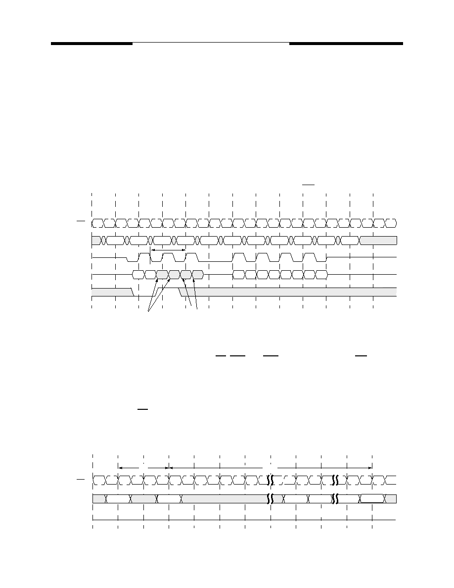
Write Interrupted by a Read
A Burst Write can be interrupted by a Read command to any bank. If a burst write operation is interrupted
prior to the end of the burst operation, then the last two pieces of input data prior to the Read command must
be masked off with the data mask (DM) input pin to prevent invalid data from being written into the memory
array. Any data that is present on the DQ pins coincident with or following the Read command will be masked
off by the Read command and will not be written to the array. The memory controller must give up control of
both the DQ bus and the DQS bus at least one clock cycle before the read data appears on the outputs in
order to avoid contention. In order to avoid data contention within the device, a delay is required (t
WTR) from
the last valid data input before a Read command can be issued to the device. It is illegal to interrupt a Write
with autoprecharge command with a Read command.
Write Interrupted by a Read Command Timing
Auto Refresh
The Auto Refresh command is issued by having CS, RAS, and CAS held low with CKE and WE high at the
rising edge of the clock. All banks must be precharged and idle for a t
RP(min) before the Auto Refresh com-
mand is applied. No control of the address pins is required once this cycle has started because of the internal
address counter. When the Auto Refresh cycle has completed, all banks will be in the idle state. A delay be-
tween the Auto Refresh command and the next Activate command or subsequent Auto Refresh command
must be greater than or equal to the t
RFC(min). Commands may not be issued to the device once an Auto
Refresh cycle has begun. CS input must remain high during the refresh period or NOP commands must be
registered on each rising edge of the CK input until the refresh period is satisfied.
Auto Refresh Timing
(CAS Latency = 2; Burst Length = 8)
T0
T1
T2
T3
T4
T5
T6
T7
T8
T9
T10
T11
Write
NOP
Read
NOP
CK, CK
Command
DQS
T12
DM
D2 D3 D4 D5
D0
D2 D3 D4 D5 D6
D1
D7
DQ
Data is masked
by Read command
Data is masked
by DM input
DQS input ignored
D0 D1
tWTR
T0
T1
T2
T3
T4
T5
T6
T7
T8
T9
T10
NOP
CK, CK
Command
CKE
T11
Auto Ref
ANY
High
Pre All
tRFC
tRP
相关PDF资料 |
PDF描述 |
|---|---|
| V58C2128404SCLJ5 | 32M X 4 DDR DRAM, 0.65 ns, PBGA60 |
| V58C2256324SAH-36 | 8M X 32 DDR DRAM, 0.55 ns, PBGA144 |
| V58C2256404SBJ5 | 64M X 4 DDR DRAM, 0.65 ns, PBGA60 |
| V58C2256164SBLJ5B | 16M X 16 DDR DRAM, 0.65 ns, PBGA60 |
| V58C2256404SCLS7I | 64M X 4 DDR DRAM, 0.75 ns, PBGA60 |
相关代理商/技术参数 |
参数描述 |
|---|---|
| V58C2128404S | 制造商:MOSEL 制造商全称:MOSEL 功能描述:HIGH PERFORMANCE 2.5 VOLT 128 Mbit DDR SDRAM |
| V58C2128804S | 制造商:MOSEL 制造商全称:MOSEL 功能描述:HIGH PERFORMANCE 2.5 VOLT 128 Mbit DDR SDRAM |
| V58C2256 | 制造商:MOSEL 制造商全称:MOSEL 功能描述:HIGH PERFORMANCE 2.5 VOLT 256 Mbit DDR SDRAM |
| V58C2256164S | 制造商:MOSEL 制造商全称:MOSEL 功能描述:HIGH PERFORMANCE 2.5 VOLT 256 Mbit DDR SDRAM |
| V58C2256324SAB30 | 制造商:Marvell 功能描述:Marvell V58C2256324SAB30 |
发布紧急采购,3分钟左右您将得到回复。