- 您现在的位置:买卖IC网 > PDF目录202172 > V58C2128164SBLS7 (PROMOS TECHNOLOGIES INC) 8M X 16 DDR DRAM, 0.75 ns, PBGA60 PDF资料下载
参数资料
| 型号: | V58C2128164SBLS7 |
| 厂商: | PROMOS TECHNOLOGIES INC |
| 元件分类: | DRAM |
| 英文描述: | 8M X 16 DDR DRAM, 0.75 ns, PBGA60 |
| 封装: | MO-233, FBGA-60 |
| 文件页数: | 2/62页 |
| 文件大小: | 977K |
| 代理商: | V58C2128164SBLS7 |
第1页当前第2页第3页第4页第5页第6页第7页第8页第9页第10页第11页第12页第13页第14页第15页第16页第17页第18页第19页第20页第21页第22页第23页第24页第25页第26页第27页第28页第29页第30页第31页第32页第33页第34页第35页第36页第37页第38页第39页第40页第41页第42页第43页第44页第45页第46页第47页第48页第49页第50页第51页第52页第53页第54页第55页第56页第57页第58页第59页第60页第61页第62页
10
V58C2128(804/404/164)SB Rev. 1.1 March 2004
ProMOS TECHNOLOGIES
V58C2128(804/404/164)SB
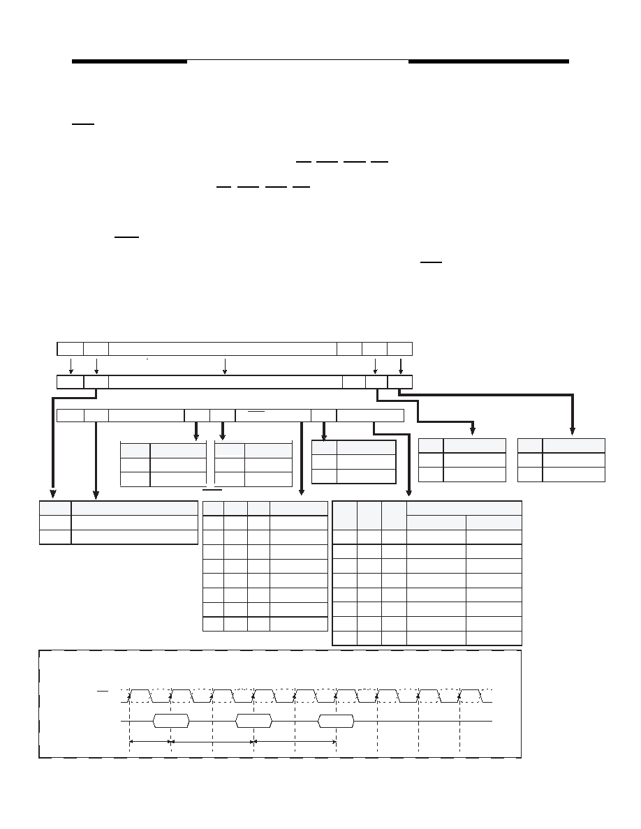
Mode Register Set (MRS)
The mode register stores the data for controlling the various operating modes of DDR SDRAM. It programs
CAS latency, addressing mode, burst length, test mode, DLL reset and various vendor specific options to
make DDR SDRAM useful for a variety of different applications. The default value of the mode register is not
defined, therefore the mode register must be written after EMRS setting for proper DDR SDRAM operation.
The mode register is written by asserting low on CS, RAS, CAS, WE and BA0 (The DDR SDRAM should be
in all bank precharge with CKE already high prior to writing into the mode register). The state of address pins
A0 ~ A11 in the same cycle as CS, RAS, CAS, WE and BA0 low is written in the mode register. Two clock
cycles are required to meet tMRD spec. The mode register contents can be changed using the same com-
mand and clock cycle requirements during operation as long as all banks are in the idle state. The mode reg-
ister is divided into various fields depending on functionality. The burst length uses A0 ~ A2, addressing mode
uses A3, CAS latency (read latency from column address) uses A4 ~ A6. A7 is a ProMOS specific test mode
during production test. A8 is used for DLL reset. A7 must be set to low for normal MRS operation. Refer to
the table for specific codes for various burst length, addressing modes and CAS latencies.
1.
MRS can be issued only at all banks precharge state.
2.
Minimum tRP is required to issue MRS command.
Address Bus
CAS Latency
A6
A5
A4
Latency
0
Reserve
0
1
Reserve
01
0
2
01
1
3
1
0
Reserve
10
1
0
2.5
1
Reserve
Burst Length
A2
A1
A0
Latency
Sequential
Interleave
0
Reserve
00
1
2
01
0
4
01
1
8
1
0
Reserve
1
0
1
Reserve
1
0
Reserve
1
Reserve
A
7
mode
0
Normal
1
Test
A3
Burst Type
0
Sequential
1
Interleave
* RFU(Reserved for future use)
should stay "0" during MRS
cycle.
A8
DLL Reset
0No
1
Yes
Mode Register Set
0
RFU : Must be set "0"
Extended Mode Register
Mode Register
DLL
I/O
A0
DLL Enable
0
Enable
1
Disable
A1
I/O Strength
0
Full
1
Half
BA0
An ~ A0
0
(Existing)MRS Cycle
1
Extended Funtions(EMRS)
Command
2
01
5
34
8
67
CK, CK
tCK
tMRD
Precharge
All Banks
Mode
Register Set
tRP*2
*1
Any
Command
BA1
BA 0
A3
A2
A1
A0
0TM
CAS Latency
BT
Burst Length
RFU
DLL
MRS
A11
to
0
相关PDF资料 |
PDF描述 |
|---|---|
| V58C2128404SCLJ5 | 32M X 4 DDR DRAM, 0.65 ns, PBGA60 |
| V58C2256324SAH-36 | 8M X 32 DDR DRAM, 0.55 ns, PBGA144 |
| V58C2256404SBJ5 | 64M X 4 DDR DRAM, 0.65 ns, PBGA60 |
| V58C2256164SBLJ5B | 16M X 16 DDR DRAM, 0.65 ns, PBGA60 |
| V58C2256404SCLS7I | 64M X 4 DDR DRAM, 0.75 ns, PBGA60 |
相关代理商/技术参数 |
参数描述 |
|---|---|
| V58C2128404S | 制造商:MOSEL 制造商全称:MOSEL 功能描述:HIGH PERFORMANCE 2.5 VOLT 128 Mbit DDR SDRAM |
| V58C2128804S | 制造商:MOSEL 制造商全称:MOSEL 功能描述:HIGH PERFORMANCE 2.5 VOLT 128 Mbit DDR SDRAM |
| V58C2256 | 制造商:MOSEL 制造商全称:MOSEL 功能描述:HIGH PERFORMANCE 2.5 VOLT 256 Mbit DDR SDRAM |
| V58C2256164S | 制造商:MOSEL 制造商全称:MOSEL 功能描述:HIGH PERFORMANCE 2.5 VOLT 256 Mbit DDR SDRAM |
| V58C2256324SAB30 | 制造商:Marvell 功能描述:Marvell V58C2256324SAB30 |
发布紧急采购,3分钟左右您将得到回复。