- 您现在的位置:买卖IC网 > PDF目录1971 > VNC2-64Q1B-TRAY (FTDI, Future Technology Devices International Ltd)IC USB HOST/DEVICE CTRL 64-QFN PDF资料下载
参数资料
| 型号: | VNC2-64Q1B-TRAY |
| 厂商: | FTDI, Future Technology Devices International Ltd |
| 文件页数: | 55/88页 |
| 文件大小: | 0K |
| 描述: | IC USB HOST/DEVICE CTRL 64-QFN |
| 应用说明: | Vinculum-II IO Cell Description AppNote Vinculum-II Debug Interface Description AppNote Vinculum-II IO Mux Explained AppNote Vinculum-II PWM Example AppNote Migrating Vinculum Designs AppNote |
| 标准包装: | 260 |
| 系列: | Vinculum-II |
| 控制器类型: | USB 2.0 控制器 |
| 接口: | USB,主机/设备配置,UART,SPI,PWM,闪存 256K,DMA 4CH |
| 电源电压: | 1.62 V ~ 1.98 V |
| 电流 - 电源: | 25mA |
| 工作温度: | -40°C ~ 85°C |
| 安装类型: | 表面贴装 |
| 封装/外壳: | 64-VFQFN 裸露焊盘 |
| 供应商设备封装: | 64-QFN(8x8) |
| 包装: | 托盘 |
| 其它名称: | VNC2-64Q1A-TRAY VNC2-64Q1A-TRAY-ND |
第1页第2页第3页第4页第5页第6页第7页第8页第9页第10页第11页第12页第13页第14页第15页第16页第17页第18页第19页第20页第21页第22页第23页第24页第25页第26页第27页第28页第29页第30页第31页第32页第33页第34页第35页第36页第37页第38页第39页第40页第41页第42页第43页第44页第45页第46页第47页第48页第49页第50页第51页第52页第53页第54页当前第55页第56页第57页第58页第59页第60页第61页第62页第63页第64页第65页第66页第67页第68页第69页第70页第71页第72页第73页第74页第75页第76页第77页第78页第79页第80页第81页第82页第83页第84页第85页第86页第87页第88页
59
Copyright 2009-2011 Future Technology Devices International Limited
Datasheet
Vinculum-II Embedded Dual USB Host Controller IC
Version 1.5
Document No.: FT_000138 Clearance No.: FTDI# 143
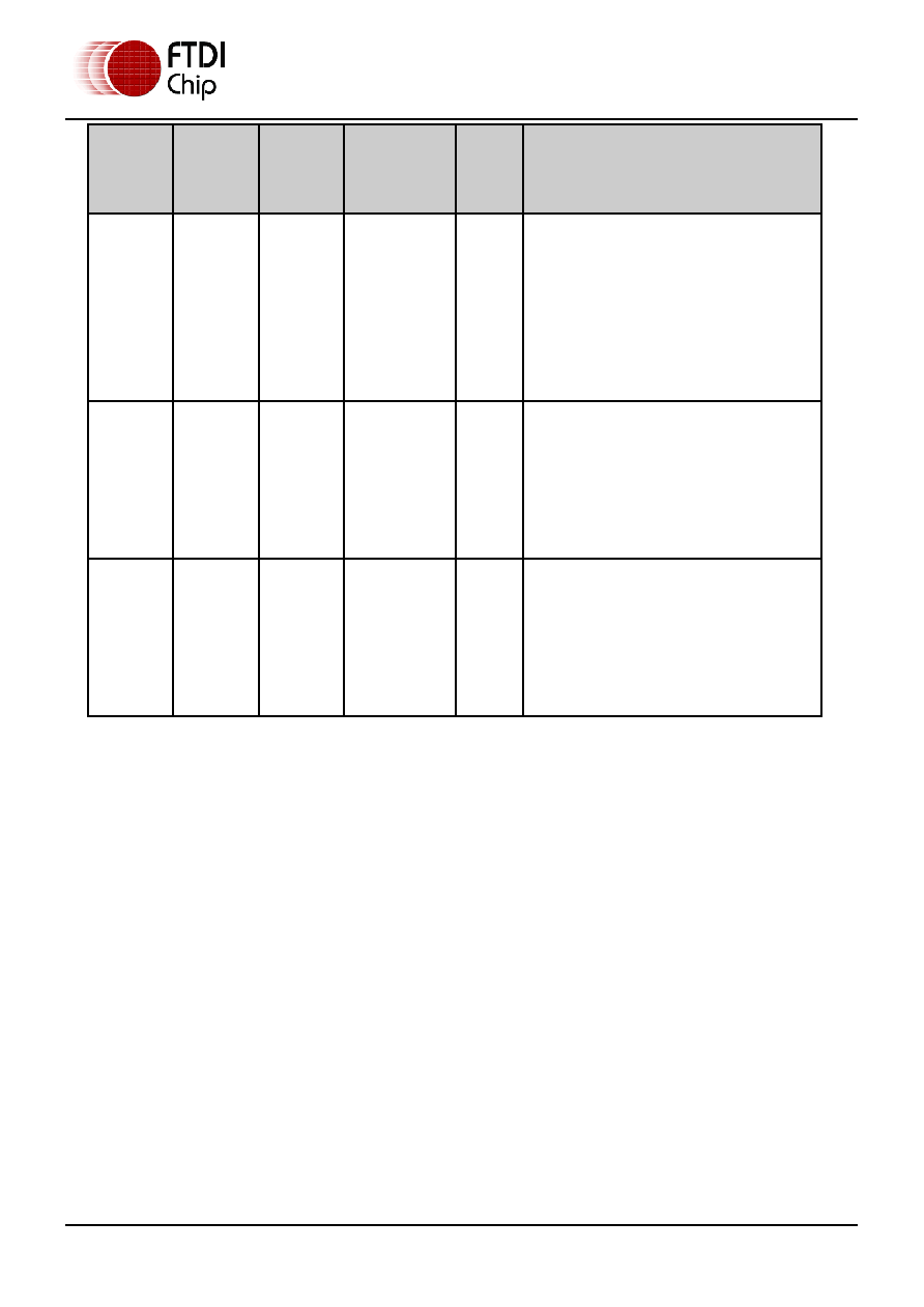
64 Pin
Package
Available
pins
48 Pin
Package
Available
pins
32 Pin
Package
Available
pins
Name
Type
Description
12, 16,
20, 25,
29, 40,
44, 48,
52, 58,
62
12,16,
21, 32,
36, 42,
46
12, 24,
30
fifo_txe#
Output
When high, do not write data into the FIFO.
When low, data can be written into the FIFO
by strobing fifo_wr# high, then low.
13, 17,
22, 26,
31, 41,
45, 49,
55, 59,
63
13, 18,
22, 33,
37, 43,
47
14, 25,
31
fifo_rd#
Input
Enables the current FIFO data byte on
D0...D7 when low. Fetches the next FIFO
data byte (if available) from the receive
FIFO buffer when fifo_rd# goes from high to
low
14, 18,
23, 27,
32, 42,
46, 50,
56, 60,
64
14, 19,
23, 34,
38, 44,
48
15, 26,
32
fifo_wr#
Input
Writes the data byte on the D0...D7 pins
into the transmit FIFO buffer when fifo_wr#
goes from high to low.
Table 6.16 Data and Control Bus Signal Mode Options - Parallel FIFO Interface
6.6.2 Read / Write Transaction Asynchronous FIFO Mode
When in Asynchronous FIFO interface mode, the timing of read and write operations on the FIFO
interface are shown in Figure 6.22 and Table 6.17.
In asynchronous mode an external device can control data transfer driving FIFO_WR# and FIFO_RD#
inputs. In contrast to synchronous mode, in asynchronous mode the 245 FIFO module generates the
output enable EN# signal. EN# signal is effectively the read signal RD#.
Current byte is available to be read when FIFO_RD# goes low. When FIFO_RD# goes high, FIFO_RXF#
output will also go high. It will only become low again when there is another byte to read.
When FIFO_WR# goes low FIFO_TXE# flag will always go high. FIFO_TXE# goes low again only when
there is still space for data to be written in to the module.
相关PDF资料 |
PDF描述 |
|---|---|
| W78E858A40FL | IC MCU 8-BIT 32K FLASH 44-PQFP |
| W83303AG | IC ACPI CONTROLLER 48-LQFP |
| W83627UHG | IC I/O CONTROLLER 128-QFP |
| W83L951DG | IC EMBEDDED CNTRLR 128-LQFP |
| X90100M8IZT1 | IC DIGITAL CAPACITOR NV 8-MSOP |
相关代理商/技术参数 |
参数描述 |
|---|---|
| VNC2DEBUGMODULE | 制造商:Future Technology Devices International (FTDI Chip) 功能描述:VNC2 Vinculum Debug Module |
| VNC712B-N50A-5TZ | 制造商:SMC Corporation of America 功能描述:Valve, media, coolant, 2 way |
| VNC-DK4-C1404CM | 制造商:L-com Inc 功能描述:4CH DVR w/4 CMOS CAMERAS no HD |
| VNC-DK4-C1404CM-HD | 制造商:L-com Inc 功能描述:4CH DVR w/4 CMOS CAMS 500GB HD |
| VNC-DK4-C2404CM | 制造商:L-com Inc 功能描述:4CH DVR w/4 CMOS CAMERAS no HD |
发布紧急采购,3分钟左右您将得到回复。