- 您现在的位置:买卖IC网 > PDF目录225534 > W28J320TT90L (WINBOND ELECTRONICS CORP) 2M X 16 FLASH 2.7V PROM, 90 ns, PDSO48 PDF资料下载
参数资料
| 型号: | W28J320TT90L |
| 厂商: | WINBOND ELECTRONICS CORP |
| 元件分类: | PROM |
| 英文描述: | 2M X 16 FLASH 2.7V PROM, 90 ns, PDSO48 |
| 封装: | 12 X 20 MM, TSOP-48 |
| 文件页数: | 6/48页 |
| 文件大小: | 1513K |
| 代理商: | W28J320TT90L |
第1页第2页第3页第4页第5页当前第6页第7页第8页第9页第10页第11页第12页第13页第14页第15页第16页第17页第18页第19页第20页第21页第22页第23页第24页第25页第26页第27页第28页第29页第30页第31页第32页第33页第34页第35页第36页第37页第38页第39页第40页第41页第42页第43页第44页第45页第46页第47页第48页
W28J320B/T
- 14 -
device (Permanent Lock) or block within the device (Block Lock) to be locked. The Clear Block Lock-
Bits command requires the command and address within the device.
The CUI does not occupy an addressable memory location. A write occurs when #WE and #CE are
active. The address and data needed to execute a command are latched on the rising edge of #WE or
#CE, whichever occurs first. Standard microprocessor write timings are used.
Figures 18 and 19 illustrate #WE and #CE controlled write operations.
9. COMMAND DEFINITIONS
When VPP ≤ VPPLK, read operations from the status register, identifier codes, or blocks are enabled.
Setting VPPH1/2 = VPP enables successful block erase, full chip erase, word/byte write and lock-bit
configuration operations.
Device operations are selected by writing specific commands into the CUI. Table 3 defines these
commands.
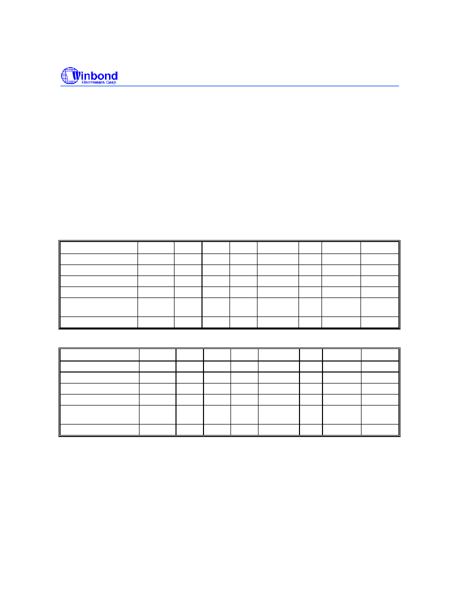
Table 2.1. Bus Operations (#BYTE = VIH) (note 1, 2)
MODE
#RESET
#CE
#OE
#WE
ADDRESS
VPP
DQ0
15 RY/#BY(3)
Read (note 8)
VIH
VIL
VIH
X
DOUT
X
Output Disable
VIH
VIL
VIH
X
High Z
X
Standby
VIH
X
High Z
X
Reset (note 4)
VIL
X
High Z
Read Identifier Codes
(note 8)
VIH
VIL
VIH
See
Figure 4, 5
X
Note 5
High Z
Write (note 6, 7, 8)
VIH
VIL
VIH
VIL
X
DIN
X
Table 2.2. Bus Operations (#BYTE = VIL) (note 1, 2)
MODE
#RESET
#CE
#OE
#WE
ADDRESS
VPP
DQ0
7
RY/#BY(3)
Read (note 8)
VIH
VIL
VIH
X
DOUT
X
Output Disable
VIH
VIL
VIH
X
High Z
X
Standby
VIH
X
High Z
X
Reset (note 4)
VIL
X
High Z
Read Identifier Codes
(note 8)
VIH
VIL
VIH
See
Figure 4,5
X
Note 5
High Z
Write (note 6, 7, 8)
VIH
VIL
VIH
VIL
X
DIN
X
Notes:
1. Refer to DC Characteristics. When VPP ≤ VPPLK, memory contents can be read, but not altered.
2. X can be VIL or VIH for control pins and addresses, and VPPLK or VPPH1/2 for VPP. See DC Characteristics for VPPLK voltages.
3. RY/#BY is VOL when the WSM is executing internal block erase, full chip erase, word/byte write or lock-bit configuration
algorithms. It is High Z during when the WSM is not busy, in block erase suspend mode (with word/byte write inactive),
word/byte write suspend mode or reset mode.
4. #RESET at VSS ±0.2V ensures the lowest power consumption.
5. See Read Identifier Codes Command section for details.
6. Command writes involving block erase, full chip erase, word/byte write or lock-bit configuration are reliably executed when VPP
= VPPH1/2 and VDD = 2.7V to 3.6V.
7. Refer to Table 3 for valid DIN during a write operation.
8. Never hold #OE low and #WE low at the same timing.
相关PDF资料 |
PDF描述 |
|---|---|
| W29S201T-45 | 128K X 16 FLASH 5V PROM, 15 ns, PDSO48 |
| W301 | PUSHBUTTON SWITCH, SPST, MOMENTARY, 10A, 28VDC, PANEL MOUNT-THREADED |
| W31-X2M5G-5 | TOGGLE SWITCH, SPST, LATCHED, 5A, 50VDC, PANEL MOUNT |
| W321-0PB-014B | T-3 1/4 SINGLE COLOR LED, SUPER BLUE, 9 mm |
| W321-0UG-048B | T-3 1/4 SINGLE COLOR LED, LIME GREEN, 9 mm |
相关代理商/技术参数 |
参数描述 |
|---|---|
| W28NK60Z | 制造商:STMICROELECTRONICS 制造商全称:STMicroelectronics 功能描述:N-CHANNEL 600 V - 0.155з - 27A TO-247 Zener-Protected SuperMESH MOSFET |
| W28-SQ11A-10 | 功能描述:CIRCUIT BREAK 10A W/SWITCH RoHS:否 类别:过电压,电流,温度装置 >> 断路器 系列:W28 标准包装:3 系列:AS168X 断路器类型:热磁动式 电压:65VDC,277/480VAC 电流 - 跳闸(It):30A 极数:3 触动器类型:按片 安装类型:DIN 轨道 其它名称:4420.02104420.0210-ND486-2338AS168X-CB3G300-NDCBE AS168X-CB3G300 |
| W28-SQ11A-15 | 制造商:TE Connectivity 功能描述: |
| W28-SQ11A-3 | 制造商:TE Connectivity 功能描述:Circuit Breaker Thermal 1Pole 3A 250VAC/32VDC |
| W28-SQ11A-5 | 制造商:TE Connectivity 功能描述:Circuit Breaker Thermal 1Pole 5A 250VAC/32VDC |
发布紧急采购,3分钟左右您将得到回复。