- 您现在的位置:买卖IC网 > PDF目录276857 > W3H128M64E2-400SBC (MICROSEMI CORP-PMG MICROELECTRONICS) DDR DRAM, PBGA208 PDF资料下载
参数资料
| 型号: | W3H128M64E2-400SBC |
| 厂商: | MICROSEMI CORP-PMG MICROELECTRONICS |
| 元件分类: | DRAM |
| 英文描述: | DDR DRAM, PBGA208 |
| 封装: | 16 X 22 MM, 1 MM PITCH, PLASTIC, BGA-208 |
| 文件页数: | 26/31页 |
| 文件大小: | 989K |
| 代理商: | W3H128M64E2-400SBC |
第1页第2页第3页第4页第5页第6页第7页第8页第9页第10页第11页第12页第13页第14页第15页第16页第17页第18页第19页第20页第21页第22页第23页第24页第25页当前第26页第27页第28页第29页第30页第31页
W3H128M64E-XSBX
4
White Electronic Designs Corporation (602) 437-1520 www.whiteedc.com
White Electronic Designs
October 2008
Rev. 1
ADVANCED
White Electronic Designs Corp. reserves the right to change products or specications without notice.
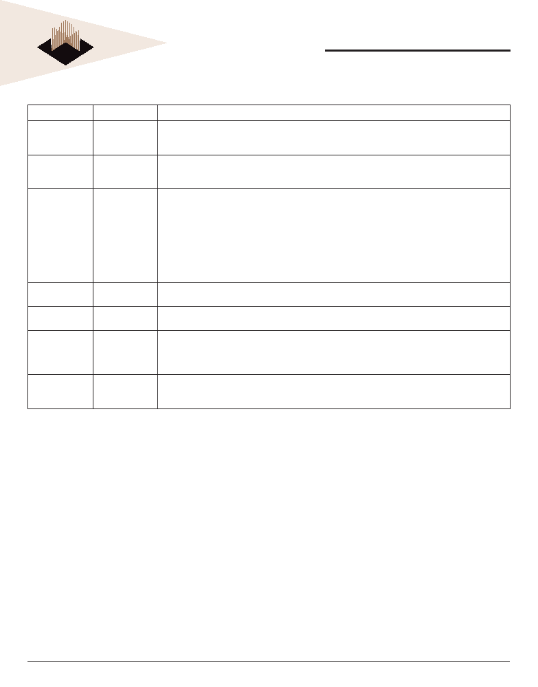
TABLE 1 – BALL DESCRIPTIONS
Symbol
Type
Description
ODT
Input
On-Die termination: ODT (registered HIGH) enables termination resistance internal to the DDR2 SDRAM. When
enabled, ODT is only applied to each of the following balls: DQ0–DQ63, LDM, UDM, LDQS, LDQS#, UDQS, and
UDQS#. The ODT input will be ignored if disabled via the LOAD MODE command.
CK, CK#
Input
Clock: CK and CK# are differential clock inputs. All address and control input signals are sampled on the crossing
of the positive edge of CK and negative edge of CK#. Output data (DQs and DQS/DQS#) is referenced to the
crossings of CK and CK#.
CKE
Input
Clock enable: CKE (registered HIGH) activates and CKE (registered LOW) deactivates clocking circuitry on the
DDR2 SDRAM. The specic circuitry that is enabled/disabled is dependent on the DDR2 SDRAM conguration
and operating mode. CKE LOW provides PRECHARGE power-down mode and SELF-REFRESH action (all banks
idle), or ACTIVE power-down (row active in any bank). CKE is synchronous for power-down entry, Power-down
exit, output disable, and for self refresh entry. CKE is asynchronous for self refresh exit. Input buffers (excluding
CKE, and ODT) are disabled during power-down. Input buffers (excluding CKE) are disabled during self refresh.
CKE is an SSTL_18 input but will detect a LVCMO SLOW level once VCC is applied during rst power-up. After
VREF has become stable during the power on and initialization sequence, it must be maintained for proper
operation of the CKE receiver. For proper SELF-REFRESH operation, VREF must be maintained.
CS#
Input
Chip select: CS# enables (registered LOW) and disables (registered HIGH) the command decoder. All commands
are masked when CS# is registered HIGH.
RAS#, CAS#,
WE#
Input
Command inputs: RAS#, CAS#, WE# (along with CS#) dene the command being entered.
LDM, UDM
Input
Input data mask: DM is an input mask signal for write data. Input data is masked when DM is concurrently sampled
HIGH during a WRITE access. DM is sampled on both edges of DQS. Although DM balls are input-only, the DM
loading is designed to match that of DQ and DQS balls. LDM is DM for lower byte DQ0–DQ7 and UDM is DM for
upper byte DQ8–DQ15, of each of U1-U4
BA0–BA2
Input
Bank address inputs: BA0–BA2 dene to which bank an ACTIVE, READ, WRITE, or PRECHARGE command is
being applied. BA0–BA2 dene which mode register including MR, EMR, EMR(2), and EMR(3) is loaded during the
LOAD MODE command.
Continued on next page
相关PDF资料 |
PDF描述 |
|---|---|
| W3HG264M72EER806AD7MG | 128M X 72 DDR DRAM MODULE, DMA244 |
| W7NCF01GH21ISBCG | 64M X 16 FLASH 3.3V PROM CARD, 150 ns, UUC |
| W7NCF256H30IS7DG | 16M X 16 FLASH 3.3V PROM CARD, 150 ns, UUC |
| WED3DG7266V7D1-MG | 64M X 72 SYNCHRONOUS DRAM MODULE, ZMA144 |
| WED7G385ATA33XDI25 | 192M X 16 FLASH 3.3V PROM MODULE, DMA144 |
相关代理商/技术参数 |
参数描述 |
|---|---|
| W3H128M64E-400SBI | 制造商:Microsemi Corporation 功能描述:128M X 64 DDR2, 1.8V, 400MHZ, 208PBGA COMMERICAL TEMP. - Bulk |
| W3H128M72E-400SBC | 制造商:Microsemi Corporation 功能描述:128M X 72 DDR2, 1.8V, 400MHZ, 208PBGA COMMERICAL TEMP. - Bulk |
| W3H128M72E-400SBI | 制造商:Microsemi Corporation 功能描述:128M X 72 DDR2, 1.8V, 400MHZ, 208PBGA INDUSTRIAL TEMP. - Bulk 制造商:Microsemi Corporation 功能描述:SDRAM MEMORY |
| W3H128M72E-400SBM | 制造商:Microsemi Corporation 功能描述:128M X 72 DDR2, 1.8V, 400MHZ, 208PBGA MIL-TEMP. - Bulk 制造商:Microsemi Corporation 功能描述:SDRAM MEMORY |
| W3H128M72E-533NBI | 制造商:Microsemi Corporation 功能描述:128M X 72 DDR2, 1.8V, 533MHZ, 208PBGA IND TEMP. - Bulk |
发布紧急采购,3分钟左右您将得到回复。