- 您现在的位置:买卖IC网 > PDF目录245699 > W3H128M64E2-533SBC (MICROSEMI CORP-PMG MICROELECTRONICS) DDR DRAM, PBGA208 PDF资料下载
参数资料
| 型号: | W3H128M64E2-533SBC |
| 厂商: | MICROSEMI CORP-PMG MICROELECTRONICS |
| 元件分类: | DRAM |
| 英文描述: | DDR DRAM, PBGA208 |
| 封装: | 16 X 22 MM, 1 MM PITCH, PLASTIC, BGA-208 |
| 文件页数: | 2/31页 |
| 文件大小: | 989K |
| 代理商: | W3H128M64E2-533SBC |
第1页当前第2页第3页第4页第5页第6页第7页第8页第9页第10页第11页第12页第13页第14页第15页第16页第17页第18页第19页第20页第21页第22页第23页第24页第25页第26页第27页第28页第29页第30页第31页
W3H128M64E-XSBX
10
White Electronic Designs Corporation (602) 437-1520 www.whiteedc.com
White Electronic Designs
October 2008
Rev. 1
ADVANCED
White Electronic Designs Corp. reserves the right to change products or specications without notice.
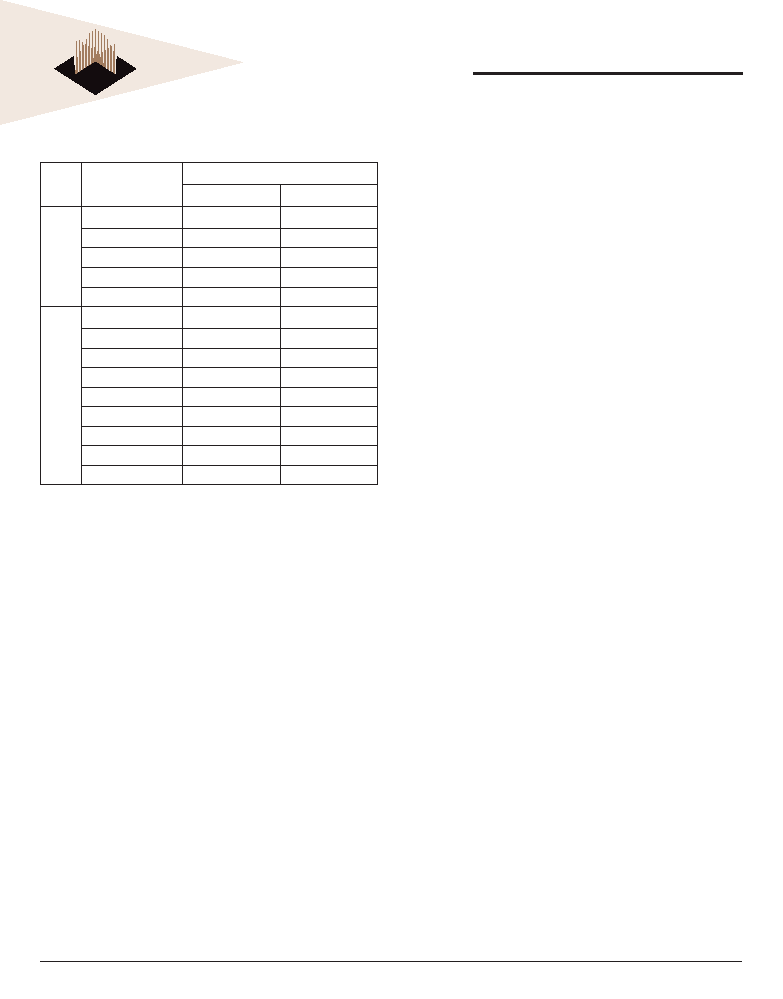
TABLE 2 – BURST DEFINITION
NOTES:
1.
For a burst length of two, A1-Ai select two-data-element block; A0 selects the
starting column within the block.
2.
For a burst length of four, A2-Ai select four-data-element block; A0-1 select the
starting column within the block.
3.
For a burst length of eight, A3-Ai select eight-data-element block; A0-2 select the
starting column within the block.
4.
Whenever a boundary of the block is reached within a given sequence above, the
following access wraps within the block.
Burst
Length
Starting Column
Address
Order of Accesses Within a Burst
Type = Sequential
Type = Interleaved
4
A1
A0
0
0-1-2-3
0
1
1-2-3-0
1-0-3-2
1
0
2-3-0-1
1
3-0-1-2
3-2-1-0
8
A2
A1
A0
0
0-1-2-3-4-5-6-7
0
1
1-2-3-0-5-6-7-4
1-0-3-2-5-4-7-6
0
1
0
2-3-0-1-6-7-4-5
0
1
3-0-1-2-7-4-5-6
3-2-1-0-7-6-5-4
1
0
4-5-6-7-0-1-2-3
1
0
1
5-6-7-4-1-2-3-0
5-4-7-6-1-0-3-2
1
0
6-7-4-5-2-3-0-1
1
7-4-5-6-3-0-1-2
7-6-5-4-3-2-1-0
OPERATING MODE
The normal operating mode is selected by issuing a
command with bit M7 set to “0,” and all other bits set to
the desired values, as shown in Figure 5. When bit M7 is
“1,” no other bits of the mode register are programmed.
Programming bit M7 to “1” places the DDR2 SDRAM into a
test mode that is only used by the manufacturer and should
not be used. No operation or functionality is guaranteed
if M7 bit is ‘1.’
DLL RESET
DLL RESET is dened by bit M8, as shown in Figure 5.
Programming bit M8 to “1” will activate the DLL RESET
function. Bit M8 is self-clearing, meaning it returns back
to a value of “0” after the DLL RESET function has been
issued.
Anytime the DLL RESET function is used, 200 clock cycles
must occur before a READ command can be issued to
allow time for the internal clock to be synchronized with
the external clock. Failing to wait for synchronization
to occur may result in a violation of the tAC or tDQSCK
parameters.
WRITE RECOVERY
Write recovery (WR) time is dened by bits M9–M11, as
shown in Figure 5. The WR register is used by the DDR2
SDRAM during WRITE with auto precharge operation.
During WRITE with auto precharge operation, the DDR2
SDRAM delays the internal auto precharge operation by
WR clocks (programmed in bits M9–M11) from the last
data burst.
WR values of 2, 3, 4, 5, or 6 clocks may be used for
programming bits M9–M11. The user is required to
program the value of WR, which is calculated by dividing
t
WR (in ns) by tCK (in ns) and rounding up a non integer
value to the next integer; WR [cycles] = tWR [ns] / tCK [ns].
Reserved states should not be used as unknown operation
or incompatibility with future versions may result.
POWER-DOWN MODE
Active power-down (PD) mode is dened by bit M12,
as shown in Figure 5. PD mode allows the user to
determine the active power-down mode, which determines
performance versus power savings. PD mode bit M12 does
not apply to precharge PD mode.
When bit M12 = 0, standard active PD mode or “fast-exit”
active PD mode is enabled. The tXARD parameter is used
for fast-exit active PD exit timing. The DLL is expected to
be enabled and running during this mode.
When bit M12 = 1, a lower-power active PD mode or “slow-
exit” active PD mode is enabled. The tXARD parameter is
used for slow-exit active PD exit timing. The DLL can be
enabled, but “frozen” during active PD mode since the exit-
to-READ command timing is relaxed. The power difference
expected between PD normal and PD low-power mode is
dened in the ICC table.
相关PDF资料 |
PDF描述 |
|---|---|
| W7NCF01GH21IS8CG | 64M X 16 FLASH 3.3V PROM CARD, 150 ns, UUC |
| W7NCF256H30CS6BG | 16M X 16 FLASH 3.3V PROM CARD, 150 ns, UUC |
| W7NCF256H30IS4BG | 16M X 16 FLASH 3.3V PROM CARD, 150 ns, UUC |
| WED7G127ATA33XDI25 | 64M X 16 FLASH 3.3V PROM MODULE, DMA144 |
| WED7G256ATA33XDI25 | 128M X 16 FLASH 3.3V PROM MODULE, DMA144 |
相关代理商/技术参数 |
参数描述 |
|---|---|
| W3H128M64E-400SBI | 制造商:Microsemi Corporation 功能描述:128M X 64 DDR2, 1.8V, 400MHZ, 208PBGA COMMERICAL TEMP. - Bulk |
| W3H128M72E-400SBC | 制造商:Microsemi Corporation 功能描述:128M X 72 DDR2, 1.8V, 400MHZ, 208PBGA COMMERICAL TEMP. - Bulk |
| W3H128M72E-400SBI | 制造商:Microsemi Corporation 功能描述:128M X 72 DDR2, 1.8V, 400MHZ, 208PBGA INDUSTRIAL TEMP. - Bulk 制造商:Microsemi Corporation 功能描述:SDRAM MEMORY |
| W3H128M72E-400SBM | 制造商:Microsemi Corporation 功能描述:128M X 72 DDR2, 1.8V, 400MHZ, 208PBGA MIL-TEMP. - Bulk 制造商:Microsemi Corporation 功能描述:SDRAM MEMORY |
| W3H128M72E-533NBI | 制造商:Microsemi Corporation 功能描述:128M X 72 DDR2, 1.8V, 533MHZ, 208PBGA IND TEMP. - Bulk |
发布紧急采购,3分钟左右您将得到回复。