- 您现在的位置:买卖IC网 > PDF目录245699 > W3H128M64E2-533SBC (MICROSEMI CORP-PMG MICROELECTRONICS) DDR DRAM, PBGA208 PDF资料下载
参数资料
| 型号: | W3H128M64E2-533SBC |
| 厂商: | MICROSEMI CORP-PMG MICROELECTRONICS |
| 元件分类: | DRAM |
| 英文描述: | DDR DRAM, PBGA208 |
| 封装: | 16 X 22 MM, 1 MM PITCH, PLASTIC, BGA-208 |
| 文件页数: | 9/31页 |
| 文件大小: | 989K |
| 代理商: | W3H128M64E2-533SBC |
第1页第2页第3页第4页第5页第6页第7页第8页当前第9页第10页第11页第12页第13页第14页第15页第16页第17页第18页第19页第20页第21页第22页第23页第24页第25页第26页第27页第28页第29页第30页第31页
W3H128M64E-XSBX
17
White Electronic Designs Corporation (602) 437-1520 www.whiteedc.com
White Electronic Designs
October 2008
Rev. 1
ADVANCED
White Electronic Designs Corp. reserves the right to change products or specications without notice.
DESELECT
The DESELECT function (CS# HIGH) prevents new
commands from being executed by the DDR2 SDRAM.
The DDR2 SDRAM is effectively deselected. Operations
already in progress are not affected.
NO OPERATION (NOP)
The NO OPERATION (NOP) command is used to instruct
the selected DDR2 SDRAM to perform a NOP (CS# is
LOW; RAS#, CAS#, and WE are HIGH). This prevents
unwanted commands from being registered during idle
or wait states. Operations already in progress are not
affected.
LOAD MODE (LM)
The mode registers are loaded via inputs BA2–BA0, and
A12–A0. BA2–BA0 determine which mode register will
be programmed. See “Mode Register (MR)”. The LM
command can only be issued when all banks are idle, and
a subsequent execute able command cannot be issued
until tMRD is met.
BANK/ROW ACTIVATION
ACTIVE COMMAND
The ACTIVE command is used to open (or activate) a
row in a particular bank for a subsequent access. The
value on the BA2–BA0 inputs selects the bank, and the
address provided on inputs A12–A0 selects the row.
This row remains active (or open) for accesses until
a PRECHARGE command is issued to that bank. A
PRECHARGE command must be issued before opening
a different row in the same bank.
ACTIVE OPERATION
Before any READ or WRITE commands can be issued to
a bank within the DDR2 SDRAM, a row in that bank must
be opened (activated), even when additive latency is used.
This is accomplished via the ACTIVE command, which
selects both the bank and the row to be activated.
After a row is opened with an ACTIVE command, a READ
or WRITE command may be issued to that row, subject to
the tRCD specication. tRCD (MIN) should be divided by
the clock period and rounded up to the next whole number
to determine the earliest clock edge after the ACTIVE
command on which a READ or WRITE command can be
entered. The same procedure is used to convert other
specication limits from time units to clock cycles. For
example, a tRCD (MIN) specication of 20ns with a 266
MHz clock (tCK = 3.75ns) results in 5.3 clocks, rounded
up to 6.
A subsequent ACTIVE command to a different row in the
same bank can only be issued after the previous active
row has been closed (precharged). The minimum time
interval between successive ACTIVE commands to the
same bank is dened by tRC
A subsequent ACTIVE command to another bank can be
issued while the rst bank is being accessed, which results
in a reduction of total row-access overhead. The minimum
time interval between successive ACTIVE commands to
different banks is dened by tRRD
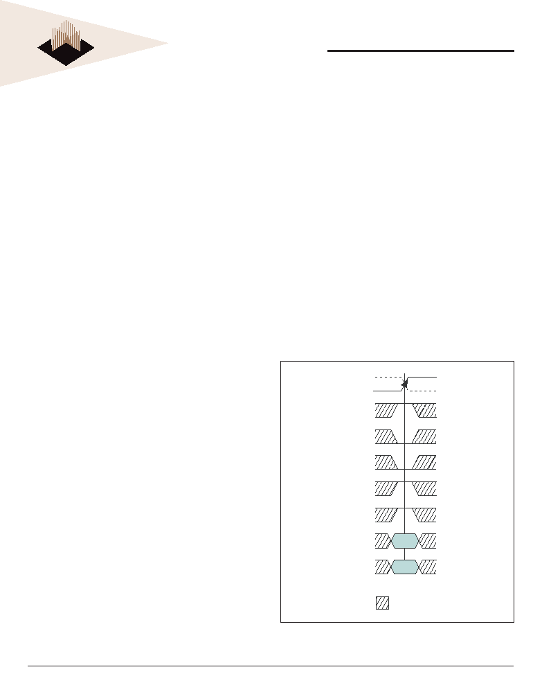
FIGURE 10 – ACTIVE COMMAND
DON’T CARE
CK
CK#
CS#
RAS#
CAS#
WE#
CKE
Row
Bank
ADDRESS
BANK ADDRESS
相关PDF资料 |
PDF描述 |
|---|---|
| W7NCF01GH21IS8CG | 64M X 16 FLASH 3.3V PROM CARD, 150 ns, UUC |
| W7NCF256H30CS6BG | 16M X 16 FLASH 3.3V PROM CARD, 150 ns, UUC |
| W7NCF256H30IS4BG | 16M X 16 FLASH 3.3V PROM CARD, 150 ns, UUC |
| WED7G127ATA33XDI25 | 64M X 16 FLASH 3.3V PROM MODULE, DMA144 |
| WED7G256ATA33XDI25 | 128M X 16 FLASH 3.3V PROM MODULE, DMA144 |
相关代理商/技术参数 |
参数描述 |
|---|---|
| W3H128M64E-400SBI | 制造商:Microsemi Corporation 功能描述:128M X 64 DDR2, 1.8V, 400MHZ, 208PBGA COMMERICAL TEMP. - Bulk |
| W3H128M72E-400SBC | 制造商:Microsemi Corporation 功能描述:128M X 72 DDR2, 1.8V, 400MHZ, 208PBGA COMMERICAL TEMP. - Bulk |
| W3H128M72E-400SBI | 制造商:Microsemi Corporation 功能描述:128M X 72 DDR2, 1.8V, 400MHZ, 208PBGA INDUSTRIAL TEMP. - Bulk 制造商:Microsemi Corporation 功能描述:SDRAM MEMORY |
| W3H128M72E-400SBM | 制造商:Microsemi Corporation 功能描述:128M X 72 DDR2, 1.8V, 400MHZ, 208PBGA MIL-TEMP. - Bulk 制造商:Microsemi Corporation 功能描述:SDRAM MEMORY |
| W3H128M72E-533NBI | 制造商:Microsemi Corporation 功能描述:128M X 72 DDR2, 1.8V, 533MHZ, 208PBGA IND TEMP. - Bulk |
发布紧急采购,3分钟左右您将得到回复。