参数资料
| 型号: | X40435V14I-CT1 |
| 厂商: | Intersil |
| 文件页数: | 16/26页 |
| 文件大小: | 0K |
| 描述: | IC VOLT MON TRPL EEPROM 14-TSSOP |
| 标准包装: | 2,500 |
| 类型: | 多压监控器 |
| 监视电压数目: | 3 |
| 输出: | 开路漏极或开路集电极 |
| 复位: | 低有效 |
| 复位超时: | 可调节/可选择 |
| 电压 - 阀值: | 1V,2.9V,4.6V |
| 工作温度: | -40°C ~ 85°C |
| 安装类型: | 表面贴装 |
| 封装/外壳: | 14-TSSOP(0.173",4.40mm 宽) |
| 供应商设备封装: | 14-TSSOP |
| 包装: | 带卷 (TR) |
�� �
�
�X40430,� X40431,� X40434,� X40435�
�SERIAL� DEVICE� ADDRESSING�
�Memory� Address� Map�
�CR,� Control� Register,� CR7:� CR0�
�Address:� 1FF� hex�
�FDR,� Fault� DetectionRegister,� FDR7:� FDR0�
�Address:� 0FF� hex�
�General� Purpose� Memory� Organization,� A8:A0�
�Address:� 000h� to� 1FFh�
�General� Purpose� Memory� Array� Configuration�
�–� last� bit� of� the� slave� command� byte� is� a� R/W� bit.� The�
�R/W� bit� of� the� Slave� Address� Byte� defines� the� oper-�
�ation� to� be� performed.� When� the� R/W� bit� is� a� one,�
�then� a� read� operation� is� selected.� A� zero� selects� a�
�write� operation.�
�Word� Address�
�The� word� address� is� either� supplied� by� the� master� or�
�obtained� from� an� internal� counter.� The� internal� counter�
�is� undefined� on� a� power-up� condition.�
�Operational� Notes�
�Memory� Address�
�A8:A0�
�000h�
�0FFh�
�100h�
�1FFh�
�Lower� 256� bytes�
�Upper� 256� bytes�
�Block� Protect� Option�
�The� device� powers-up� in� the� following� state:�
�–� The� device� is� in� the� low� power� standby� state.�
�–� The� WEL� bit� is� set� to� ‘0’.� In� this� state� it� is� not� possi-�
�ble� to� write� to� the� device.�
�–� SDA� pin� is� the� input� mode.�
�–� RESET/RESET� Signal� is� active� for� t� PURST� .�
�Slave� Address� Byte�
�Following� a� start� condition,� the� master� must� output� a�
�Slave� Address� Byte.� This� byte� consists� of� several� parts:�
�–� a� device� type� identifier� that� is� always� ‘101x’.� Where�
�x� =� 0� is� for� Array,� x� =� 1� is� for� Control� Register� or�
�Fault� Detection� Register.�
�–� next� two� bits� are� ‘0’.�
�–� next� bit� that� becomes� the� MSB� of� the� address.�
�Figure� 14.� X40430,� X40431,� X40434,� X40435�
�Addressing�
�Data� Protection�
�The� following� circuitry� has� been� included� to� prevent�
�inadvertent� writes:�
�–� The� WEL� bit� must� be� set� to� allow� write� operations.�
�–� The� proper� clock� count� and� bit� sequence� is� required�
�prior� to� the� stop� bit� in� order� to� start� a� nonvolatile�
�write� cycle.�
�–� A� three� step� sequence� is� required� before� writing� into�
�the� Control� Register� to� change� Watchdog� Timer� or�
�Block� Lock� settings.�
�General� Purpose� Memory�
�Slave� Byte�
�1� 0�
�1�
�0�
�0�
�0�
�A8� R/W�
�–� The� WP� pin,� when� held� HIGH,� prevents� all� writes� to�
�the� array� and� all� the� Register.�
�Control� Register�
�Fault� Detection� Register�
�1�
�1�
�0�
�0�
�1�
�1�
�1�
�1�
�0�
�0�
�0�
�0�
�1�
�0�
�R/W�
�R/W�
�Word� Address�
�General� Purpose� Memory� A7�
�A6� A5� A4� A3� A2� A1�
�A0�
�Control� Register�
�Fault� Detection� Register�
�1�
�1�
�1�
�1�
�1�
�1�
�1�
�1�
�1�
�1�
�1�
�1�
�1�
�1�
�1�
�1�
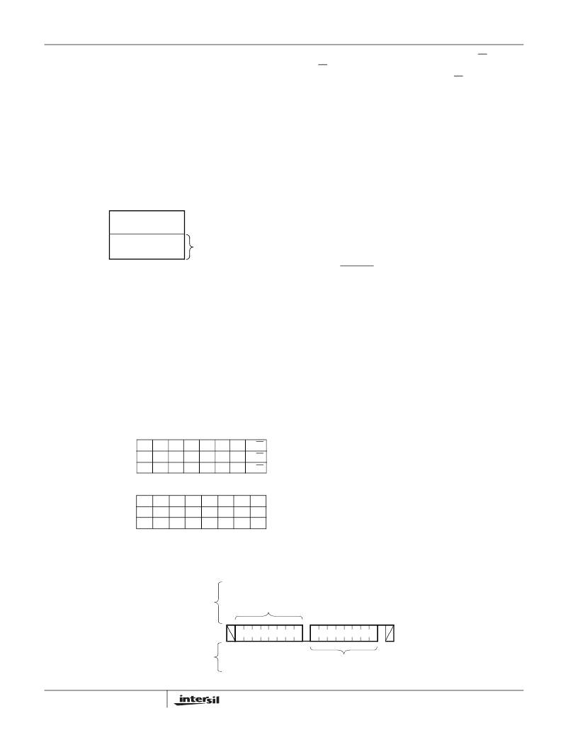
�Figure� 15.� Current� Address� Read� Sequence�
�.�
�16�
�Signals� from�
�the� Master�
�SDA� Bus�
�Signals� from�
�the� Slave�
�S�
�t�
�a�
�r�
�t�
�Slave�
�Address�
�1� 0� 1� 0� 0� 0�
�1�
�A�
�C�
�K�
�Data�
�S�
�t�
�o�
�p�
�FN8251.1�
�May� 24,� 2006�
�相关PDF资料 |
PDF描述 |
|---|---|
| X4045S8T1 | IC SUPERVISOR CPU 4K EE 8-SOIC |
| X40626V14T1 | IC SUPERVISOR CPU DUAL 14-TSSOP |
| X4165V8I-4.5A | IC SUPERVISOR CPU 16K EE 8-TSSOP |
| X4285V8I-4.5A | IC SUPERVISOR CPU 128K EE 8TSSOP |
| X4325V8I-4.5A | IC SUPERVISOR CPU 32K EE 8-TSSOP |
相关代理商/技术参数 |
参数描述 |
|---|---|
| X40435V14IZ-A | 制造商:INTERSIL 制造商全称:Intersil Corporation 功能描述:Triple Voltage Monitor with Integrated CPU Supervisor |
| X40435V14IZ-B | 制造商:INTERSIL 制造商全称:Intersil Corporation 功能描述:Triple Voltage Monitor with Integrated CPU Supervisor |
| X40435V14Z-A | 制造商:INTERSIL 制造商全称:Intersil Corporation 功能描述:Triple Voltage Monitor with Integrated CPU Supervisor |
| X40435V14Z-B | 制造商:INTERSIL 制造商全称:Intersil Corporation 功能描述:Triple Voltage Monitor with Integrated CPU Supervisor |
| X4043M8 | 功能描述:IC CPU SUPERV 4K EE RST LO 8MSOP RoHS:否 类别:集成电路 (IC) >> PMIC - 监控器 系列:- 标准包装:1 系列:- 类型:简单复位/加电复位 监视电压数目:1 输出:开路漏极或开路集电极 复位:低有效 复位超时:标准传输延迟为 60 µs 电压 - 阀值:3V 工作温度:-40°C ~ 85°C 安装类型:表面贴装 封装/外壳:SC-74A,SOT-753 供应商设备封装:SOT-23-5 包装:Digi-Reel® 其它名称:LM8364BALMF30DKR |
发布紧急采购,3分钟左右您将得到回复。